Voltage detection
Voltage detectionHardware connectionControl principlePin definitionSoftware codeControl functionExperimental phenomenon
The tutorial demonstrates ADC (ADC12_IN5) to obtain the real-time voltage of the battery pack and print the voltage value through the serial port.
The tutorial only introduces the standard library project code
Hardware connection
| Peripherals | Development board | Description |
|---|---|---|
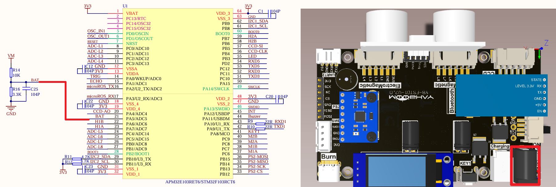
| Battery pack | PA5 | The battery pack DC interface needs to be connected to the development board |
Control principle
The converted value of the battery BAT pin is obtained through a single ADC, and the value is converted into actual voltage information and printed out through USART1.
ADC
STM32F103RCT6 has three 12-bit analog-to-digital converters embedded, and each ADC controller has up to 16 channels.
ADC channel
Only introduce the ADC channel corresponding to the battery pack interface.
| Main control chip | Pin | Main function (after reset) | Default multiplexing function | Redefine function |
|---|---|---|---|---|
| STM32F103RCT6 | PA5 | PA5 | SPI1_SCK/DAC_OUT2/ADC12_IN5 |
ADC conversion value
The ADC of STM32F103RCT6 is a 12-bit successive approximation analog-to-digital converter with 12-bit resolution;
The converted value of ADC can be stored in 16-bit data register in left-aligned or right-aligned mode.
ADC conversion mode
The A/D conversion of each ADC channel can be performed in single, continuous, scan or intermittent mode.
| Mode | Function |
|---|---|
| Single conversion mode | ADC performs only one conversion |
| Continuous conversion mode | Starts another conversion as soon as the previous ADC conversion is completed |
| Scan mode | Used to scan a group of ADC channels |
| Intermittent mode | Converts multiple ADC channels in groups until the entire sequence is converted |
xxxxxxxxxxRegular channel: Perform channel conversion in a certain orderInjection channel: The injection channel can interrupt the conversion of the regular channel to execute the injection channel, and then continue to execute the regular channel conversion after the injection channel is completed
ADC conversion time
The input clock of the ADC must not exceed 14MHz, which is generated by the frequency division of PCLK2.
Conversion time in this tutorial: ADC clock frequency 12MHz, sampling time 239.5 clock cycles
Actual voltage conversion: ADC internal reference voltage 3.3V
Referring to the hardware schematic diagram, we can see: Current equality principle
Pin definition
| Main control chip | Pin | Main function (after reset) | Default multiplexing function | Redefine function |
|---|---|---|---|---|
| STM32F103RCT6 | PA5 | PA5 | SPI1_SCK/DAC_OUT2/ADC12_IN5 |
Software code
Since the default function of the PA5 pin is a normal IO pin function, we need to use the multiplexing function.
xxxxxxxxxxProduct supporting data source code path: Attachment → Source code summary → 1.Base_Course → 6.ADC
Control function
The tutorial only briefly introduces the code, and you can open the project source code to read it in detail.
Battery_init
x//Battery power detection initializationvoid Battery_init(void){ADC_InitTypeDef ADC_InitStructure;GPIO_InitTypeDef GPIO_InitStructure;RCC_APB2PeriphClockCmd(BAT_GPIO_CLK | BAT_ADC_CLK, ENABLE); //Enable BAT_ADC channel clockRCC_ADCCLKConfig(RCC_PCLK2_Div6); //Set ADC division factor 6//72M/6=12, ADC maximum input clock cannot exceed 14M//PA5 as analog channel input pinGPIO_InitStructure.GPIO_Pin = BAT_GPIO_PIN;GPIO_InitStructure.GPIO_Mode = GPIO_Mode_AIN; //Analog inputGPIO_Init(BAT_GPIO_PORT, &GPIO_InitStructure); //Initialization GPIOA.5ADC_DeInit(BAT_ADC); //Reset BAT_ADC and reset all registers of the peripheral BAT_ADC to default valuesADC_InitStructure.ADC_Mode = ADC_Mode_Independent; //ADC independent modeADC_InitStructure.ADC_ScanConvMode = DISABLE; //Single channel modeADC_InitStructure.ADC_ContinuousConvMode = DISABLE; //Single conversion modeADC_InitStructure.ADC_ExternalTrigConv = ADC_ExternalTrigConv_None; //Conversion is started by software instead of external triggerADC_InitStructure.ADC_DataAlign = ADC_DataAlign_Right; //ADC data right alignmentADC_InitStructure.ADC_NbrOfChannel = 1; //Number of ADC channels for regular conversion in sequenceADC_Init(BAT_ADC, &ADC_InitStructure); //Initialize peripheral ADCx according to specified parametersADC_Cmd(BAT_ADC, ENABLE); //Enable specified BAT_ADCADC_ResetCalibration(BAT_ADC); //Start reset calibrationwhile (ADC_GetResetCalibrationStatus(BAT_ADC)); //Wait for reset calibration to endADC_StartCalibration(BAT_ADC); //Start AD calibrationwhile (ADC_GetCalibrationStatus(BAT_ADC)); //Wait for calibration to end}
Battery_Get
xxxxxxxxxx// Get ADC value, ch: channel valuestatic uint16_t Battery_Get(uint8_t ch){uint16_t timeout = 1000;// Set the specified ADC rule group channel, set their conversion order and sampling timeADC_RegularChannelConfig(BAT_ADC, ch, 1, ADC_SampleTime_239Cycles5);// Channel 1, the regular sampling order value is 1, and the sampling time is 239.5 cyclesADC_SoftwareStartConvCmd(BAT_ADC, ENABLE); // Enable software conversion functionwhile (!ADC_GetFlagStatus(BAT_ADC, ADC_FLAG_EOC) && timeout--); // Wait for the conversion to endreturn ADC_GetConversionValue(BAT_ADC); // Return the most recent conversion result of the BAT_ADC rule group}
Battery_Get_Average
xxxxxxxxxxuint16_t Battery_Get_Average(uint8_t ch, uint8_t times){uint16_t temp_val = 0;uint8_t t;for (t = 0; t < times; t++){temp_val += Battery_Get(ch);}if (times == 4){temp_val = temp_val >> 2;}else{temp_val = temp_val / times;}return temp_val;}
Get_Measure_Volotage
xxxxxxxxxx// Get the measured raw voltage valuefloat Get_Measure_Volotage(void){uint16_t adcx;float temp;adcx = Battery_Get(BAT_ADC_CH); // Battery channel 5 is measured oncetemp = (float)adcx * (3.30f / 4096);return temp;}
Get_Battery_Volotage
xxxxxxxxxx// Get the actual battery voltage before voltage divisionfloat Get_Battery_Volotage(void){float temp;temp = Get_Measure_Volotage();// The actual measured value is a little lower than the calculated value.temp = temp * 4.03f; //temp*(10+3.3)/3.3;return temp;}
Experimental phenomenon
The ADC.hex file generated by the project compilation is located in the OBJ folder of the ADC project. Find the ADC.hex file corresponding to the project and use the FlyMcu software to download the program to the development board.
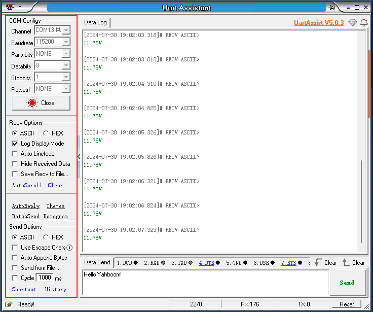
After the program is successfully downloaded: the LED switches on and off every 500ms; using the serial port debugging assistant, you can see the serial port returns the battery pack voltage information.
xxxxxxxxxxWhen using the serial port debugging assistant, you need to pay attention to the serial port settings. If the settings are wrong, the phenomenon may be inconsistent