Home
Learn
Solution
Software
∨
Controlling software
Programming software
About us
Store
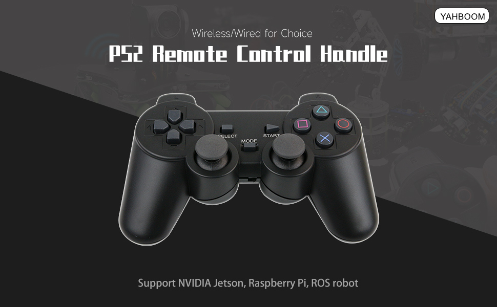
PS2 Handle(2.4GHz)
Tutorials
1. PS2 handle working Principle
2. PS2 handle use description
Download ZIP
Welcome to PS2 Handle(2.4GHz) repository
Loading...