Welcome to 8x8 matrix module repository
8x8 matrix module
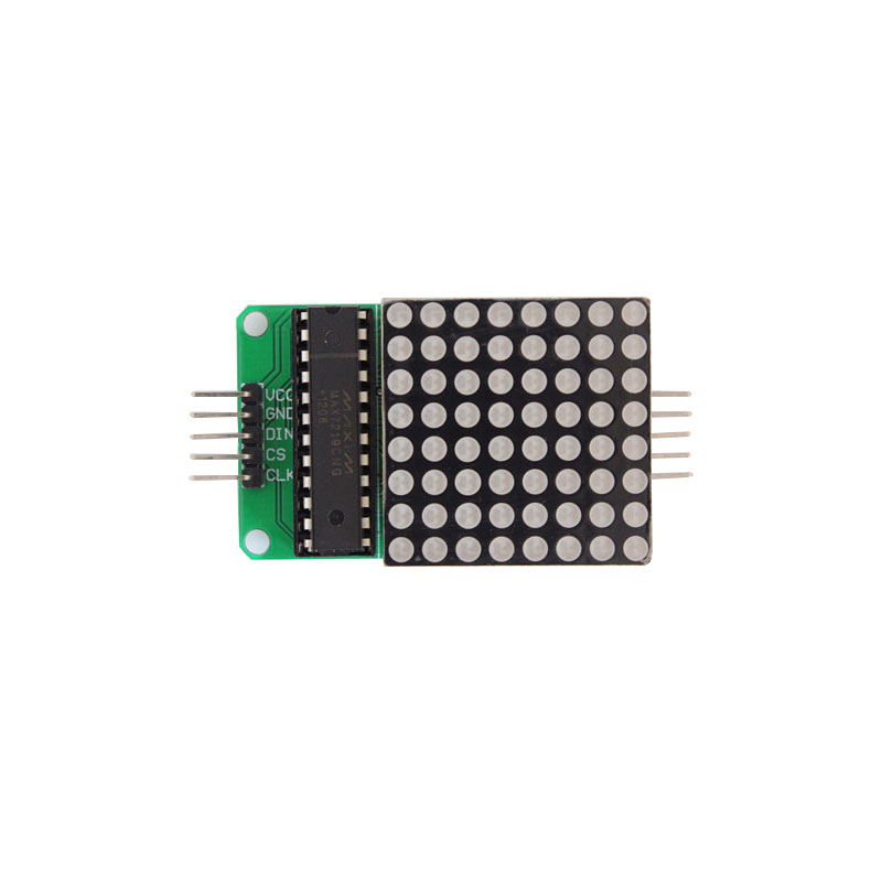
The actual object is shown below.

Introduction of 8*8 dot matrix:
This module consists of 64 LEDs with MAX7219 driver chip. It can control 64 LEDs by 16-bit data serial input and output.
The 8X8 dot matrix consists of 64 LEDs, and each LED is placed at the intersection of the row and column lines. Pins recognition: 4 sides of the dot matrix module, there is a silk screen on one side, and there is a plastic protrusion in the middle; the pin is placed down, the silk screen is facing yourself, and the left foot is the 1st foot, which is arranged counterclockwise.

Introduction of MAX7219:
The MAX7219/MAX7221 are integrated serial input/output common-cathode display drivers that can be connected to a microprocessor with an 8-bit digital 7-segment LED display, or a bar graph display, or 64 separate LEDs. The chip includes an on-chip B-type BCD encoder, multi-channel scan loop, segment word driver, and it possess a 8*8 static RAM to store each data. Only one external register is used to set the segment current of each LED.
The MAX7219 is connected to a single-chip computer with three leads (DIN, CLK, LOAD) using a 16-bit data serial shift receiver. That is, the MCU sends the 16-bit binary number bit by bit to the DIN terminal, ready before the rising edge of CLK. Each rising edge of CLK shifts one bit of data into the shift register in MAX7219. When the 16-bit data is shifted in, load 16-bit data into the corresponding location in the MAX7219 on the rising edge of the LOAD pin signal. Dynamic display is realized by the MAX7219 internal hardware dynamic scanning display control circuit.
Pins:
The MAX7219 is a 24-pin chip as shown below. The functions of each pin are as follows:
DIN: Serial data input;
DIG0~DIG7: LED bit line;
LOAD/CS: Data loading signal input;
SEGA~SEGG, SEGDp: Segment code output;
ISET: Hardware brightness adjustment terminal;
DOUT: Serial data output;
CLK: Shift pulse input terminal;
V+: Positive power supply;
GND: Ground

Serial data format:
The 16-bit address/data shift register receives serial data for serial/parallel conversion. The meaning of the 16-bit data is as follows:
D7~D0: Write data to internal RAM and function register;
D8~D11: Internal RAM and function register address;
D12~D15: No definition.
Addressable data register and control register:
(1) The internal RAM addresses 01 to 08H correspond to DIG0 to DIG7, respectively.
(2) Decoding mode register (address 09H): Each bit of the 8-bit binary number of this register controls the decoding mode of 8 LED displays. When it is high, the BCD-B decoding mode is selected, and when it is low, the non-decoding mode is selected (that is, the data is sent as a font code).
(3) Brightness register (address 0AH): Brightness can be adjusted in both hardware and software. The D0 to D3 bits in the Brightness register control the brightness of the LED display.
(4) Scan limit register (address 0BH): The D0 to D3 bit data setting value in this register is 0~7H, and the set value indicates the display dynamic scanning digits 1~8.
(5) Stop register (address 0CH): When D0=0, MAX721 is in stop state; when D0=1, it is in normal working state.
(6) Display test register (address 0FH): When D0=0, MAX7219 works normally according to the setting mode; when D0=1, it is in the test state. In this state, all LEDs are displayed at maximum brightness regardless of the mode of the MAX7219.
Timing diagram: