Welcome to MSPM0G3519 Development Board repository
9. DMA Transfer
DMA Transfer
DMA Transfer1. Learning ObjectivesDMA Principle2. Hardware Setup3. Experimental Steps1. Open SYSCONFIG Configuration Tool2. ADC Parameter Configuration3. DMA Parameter Configuration4. Write Program5. Compile4. Program Analysis5. Experimental Phenomenon
1. Learning Objectives
1.Understand basic DMA knowledge.
2.Learn basic DMA usage and display the transferred ADC data on the serial assistant.
DMA Principle
DMA (Direct Memory Access) is a technology used in computer systems that allows peripherals to directly access memory without CPU involvement to complete data transfer. It enables efficient exchange of data between peripherals (such as ADC, DAC, memory, etc.) and memory, reducing CPU burden and improving overall system performance.
Principle:
Trigger Data Transfer: DMA operations are usually triggered by external devices (such as ADC, sensors) or internal events (such as timer overflow).
Initialize DMA Controller: CPU configures parameters for the DMA controller including source address, destination address, transfer data size, transfer direction, etc.
Direct Data Transfer: Once the DMA controller is activated, it can directly transfer data from the source address (peripheral output buffer or memory) to the destination address (memory or peripheral) without CPU intervention.
Notify CPU After Transfer Complete: After DMA completes data transfer, it can send an interrupt request to the CPU, informing that data is ready or transfer has completed successfully.
2. Hardware Setup
The DMA support in these devices includes the following important features:
12 independent DMA transfer channels
12 independent DMA transfer channels
– 6 full-featured channels (DMA0-DMA5), supporting repeat transfer mode
– 6 basic channels (DMA6-DMA11), supporting single transfer mode
Configurable DMA channel priority
Byte (8-bit), short word (16-bit), word (32-bit), long word (64-bit), and ultra-long word (128-bit) or mixed byte and word transfer capability
Transfer counter block size supports transferring any type of data up to 64k
Configurable DMA transfer trigger selection
Active channel interrupt providing service for other channels
Early interrupt generation for ping-pong buffer architecture
Cascade channels when activity on another channel completes
Stride mode supporting data reorganization, such as three-phase metering applications
Collection mode
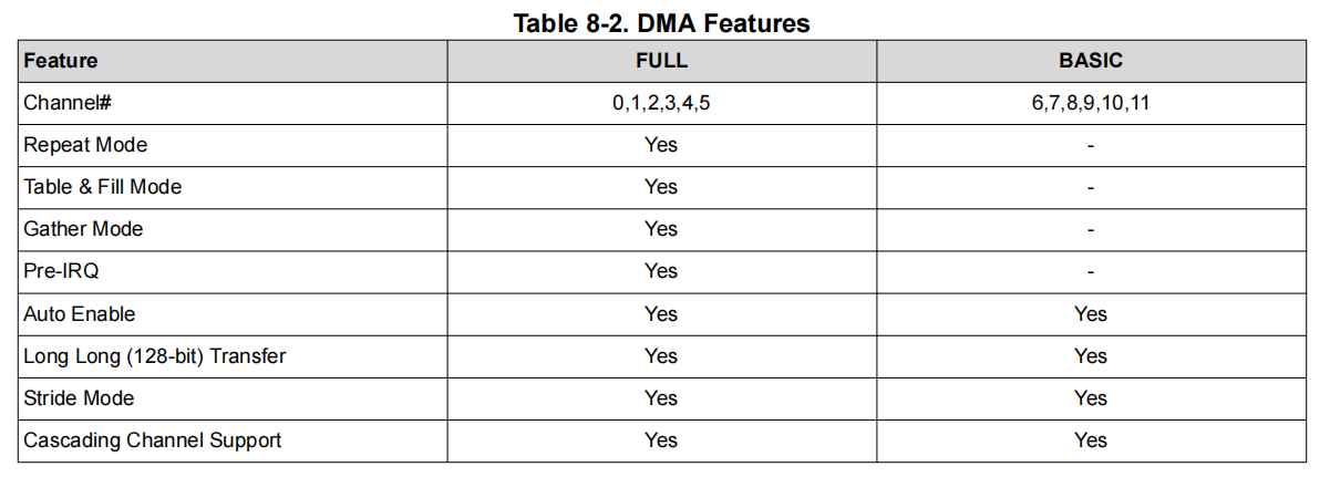
By checking the datasheet, only full-featured DMA channels support repeat transfer, early interrupt, and extended mode. Basic DMA channels support basic data transfer and interrupts, but are sufficient for simple data transfer requirements.
MSPM0G3519 DMA supports four transfer modes, each channel can be individually configured for its transfer mode. For example, channel 0 can be configured for single word or single byte transfer mode, channel 1 configured for block transfer mode, and channel 2 configured for repeat block transfer mode. Transfer modes are configured independently of addressing modes. Any addressing mode can be used with any transfer mode. Three types of data can be transferred, selected via .srcWidth and .destWidth control bits. Source and destination can be byte, short word, or word data. Transfer is also supported from byte to byte, short word to short word, word to word, or any combination. As follows:
Single word or single byte transfer: Each transfer requires a separate trigger. DMA is automatically disabled when DMAxSZ transfer has been generated.
Block transfer: An entire block will be transferred after one trigger. DMA is automatically disabled at the end of block transfer.
Repeat single word or single byte transfer: Each transfer requires a separate trigger, DMA remains enabled.
Repeat block transfer: An entire block will be transferred after one trigger, DMA remains enabled.
Based on these three modes, MSPM0G3519 provides 6 addressing methods,
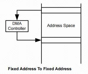
Fixed address to fixed address:
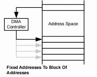
Fixed address to block address:
Block address to fixed address:
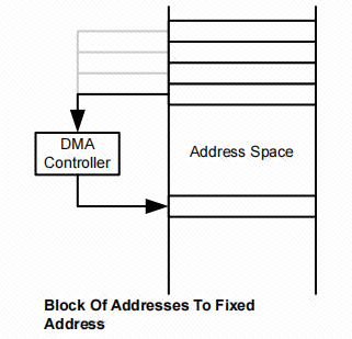
Block address to block address:
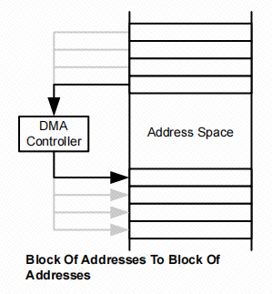
Fill data to block address:
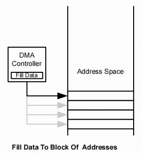
Data table to specified address:
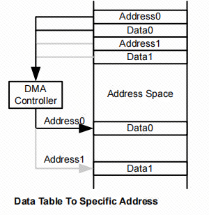
3. Experimental Steps
This case will use ADC to collect voltage from PA27 pin and use DMA to directly transfer ADC collected data to a specified address.
1. Open SYSCONFIG Configuration Tool
Open the empty project from SDK in KEIL.
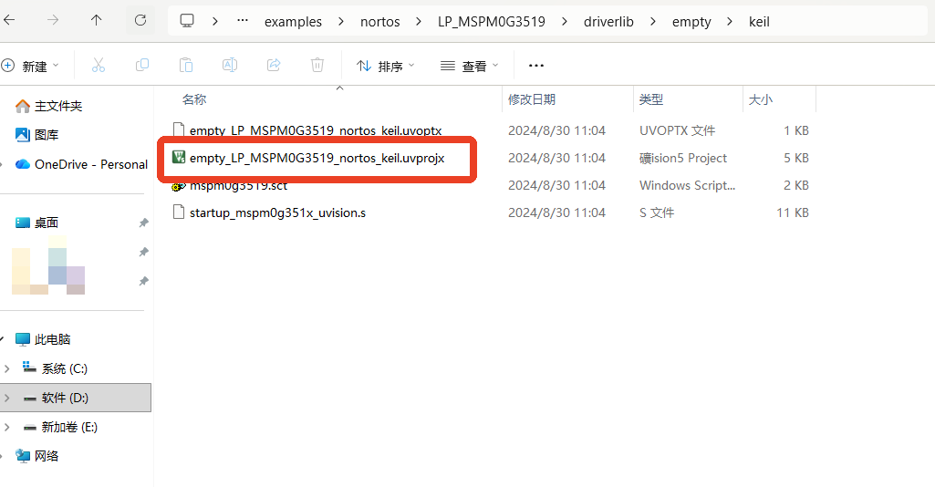
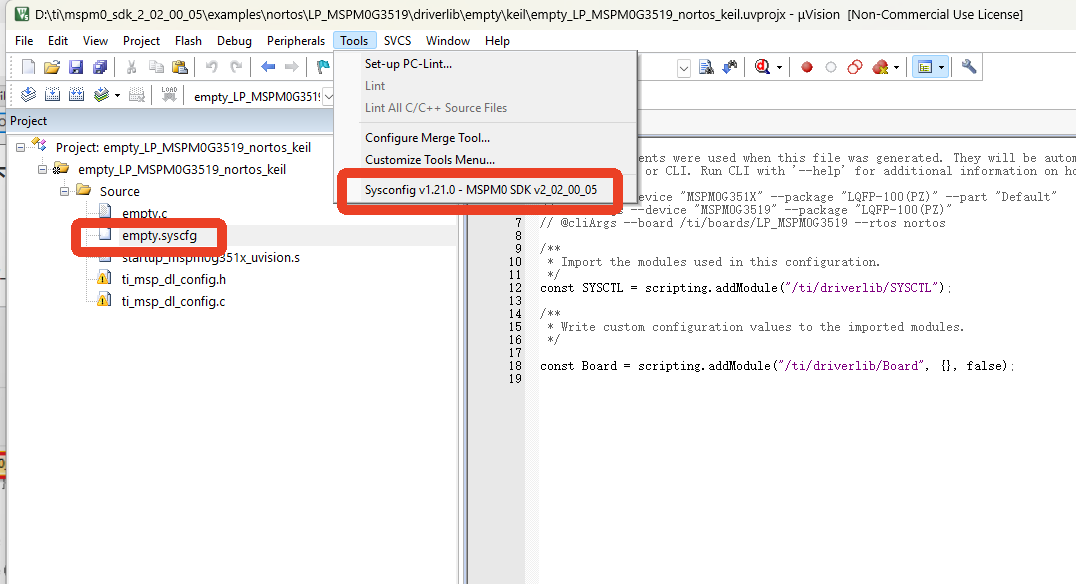
After selecting, open it. In the keil interface, open the empty.syscfg file. With the empty.syscfg file open, then open the SYSCONFIG GUI interface from the Tools menu.
2. ADC Parameter Configuration
The ADC configuration here is the same as the ADC Acquisition case.
Configure ADC resolution and interrupt. This case does not use interrupt, so nothing is selected here.

3. DMA Parameter Configuration
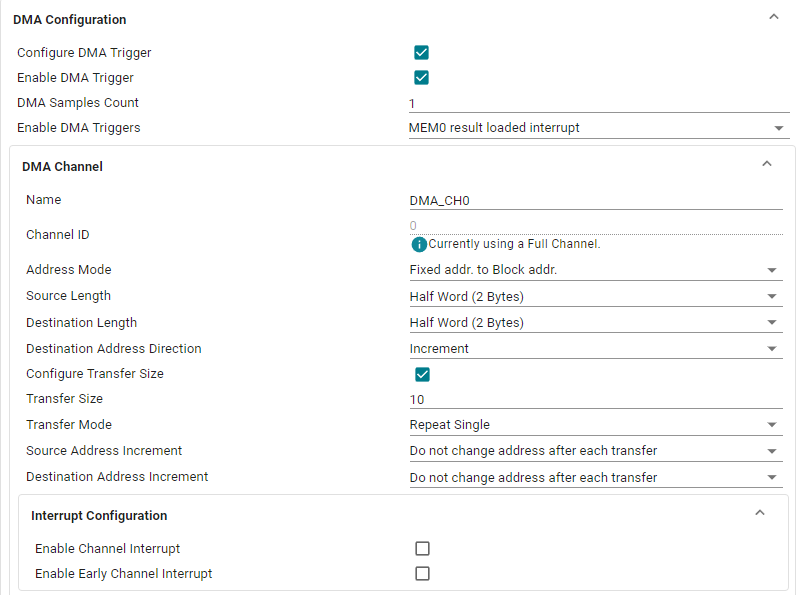
Parameter Description:
Configure DMA Trigger: Whether to enable DMA configuration function. Select enable here.
Enable DMA Trigger: Enable DMA trigger.
DMA Samples Count: DMA sample count. Set to 1.
Enable DMA Triggers: DMA trigger mode. Configure as MEM0 result loaded interrupt ADC result register 0 loaded interrupt.
Address Mode: DMA addressing mode. Configure as Fixed addr. to Block addr. Fixed address to block address.
Source Length: Source address data bit width. Configure as Half Word (2 Bytes) data bit width 2 bytes.
Destination Length: Destination address data bit width configuration. Same as above.
Destination Address Direction: Destination address direction. Select Increment, block address enables increment.
Configure Transfer size: Whether to configure transfer data amount. Select enable here.
Transfer Size: Amount of data to transfer. Configure as 10, one block transfer data amount is 10 numbers.
Transfer Mode: DMA transfer mode. Configure as Repeat Single repeat single transfer.
Source Address Increment: Whether source address increments. Disable.
Destination Address Increment: Whether destination address increments. Disable.
Enable Channel Interrupt: Whether to enable DMA channel interrupt. Disable.
Click SAVE to save the configuration in SYSCONFIG, then close SYSCONFIG and return to keil.
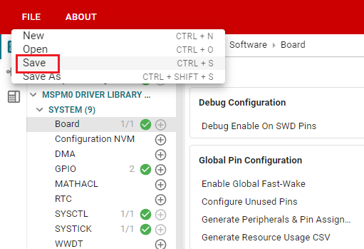
In the popup, select Yes to All
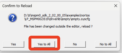
We also need to confirm whether ti_msp_dl_config.c and ti_msp_dl_config.h files are updated. Compile directly, compilation will automatically update to keil. If not updated, we can also copy the file content from SYSCONFIG.
4. Write Program
In the empty.c file, write the following code
x#include "ti_msp_dl_config.h"#include "stdio.h"
volatile unsigned int delay_times = 0;volatile bool gCheckADC; //ADC acquisition success flagvolatile uint16_t ADC_VALUE[20];
void delay_ms(unsigned int ms); //Precise millisecond delay with tick timerunsigned int adc_getValue(unsigned int number);//Read ADC data
/******************************Serial port redirection***************************************/#if !defined(__MICROLIB)//If you don't use the micro library, you need to add the following function#if (__ARMCLIB_VERSION <= 6000000)//If the compiler is AC5, define the following structurestruct __FILE{ int handle;};#endif
FILE __stdout;
//Define _sys_exit() to avoid using semihosting modevoid _sys_exit(int x){ x = x;}#endif//printf function redefinitionint fputc(int ch, FILE *stream){ //Wait when serial port 0 is busy, and send the incoming characters when it is not busy while( DL_UART_isBusy(UART_0_INST) == true );
DL_UART_Main_transmitData(UART_0_INST, ch);
return ch;}/*********************************************************************/
int main(void){ unsigned int adc_value = 0; unsigned int voltage_value = 0; int i = 0;
SYSCFG_DL_init();
//Clear the serial port interrupt flag NVIC_ClearPendingIRQ(UART_0_INST_INT_IRQN); //Enable serial port interrupt NVIC_EnableIRQ(UART_0_INST_INT_IRQN);
//Set the starting address of DMA transfer DL_DMA_setSrcAddr(DMA, DMA_CH0_CHAN_ID, (uint32_t) &ADC0->ULLMEM.MEMRES[0]); //Set the destination address of DMA transfer DL_DMA_setDestAddr(DMA, DMA_CH0_CHAN_ID, (uint32_t) &ADC_VALUE[0]); //Enable DMA DL_DMA_enableChannel(DMA, DMA_CH0_CHAN_ID); //Start ADC conversion DL_ADC12_startConversion(ADC_VOLTAGE_INST);
printf("adc_dma Demo start\r\n");
while (1) { //Get ADC data adc_value = adc_getValue(10); printf("adc value:%d\r\n", adc_value);
//Convert the data collected by ADC into voltage voltage_value = (int)((adc_value/4095.0*3.3)*100);
printf("voltage value:%d.%d%d\r\n", voltage_value/100, voltage_value/10%10, voltage_value%10 );
delay_ms(1000); }}//Delay functionvoid delay_ms(unsigned int ms){ delay_times = ms; while( delay_times != 0 );}
//Read ADC dataunsigned int adc_getValue(unsigned int number){ unsigned int gAdcResult = 0; unsigned char i = 0;
//Collect multiple times and accumulate for( i = 0; i < number; i++ ) { gAdcResult += ADC_VALUE[i]; } //Mean Filter gAdcResult /= number;
return gAdcResult;}
//Tick timer interrupt service functionvoid SysTick_Handler(void){ if( delay_times != 0 ) { delay_times--; }}5. Compile
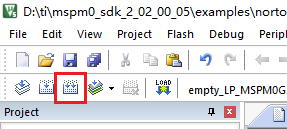
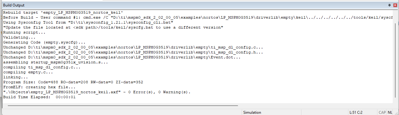
Click the Rebuild icon. The following prompt indicates compilation is complete with no errors.
4. Program Analysis
empty.c
xxxxxxxxxx//Read ADC dataunsigned int adc_getValue(unsigned int number){        unsigned int gAdcResult = 0;        unsigned char i = 0;
        //Collect multiple times and accumulate        for( i = 0; i < number; i++ )        {                gAdcResult += ADC_VALUE[i];        }        //Mean Filter        gAdcResult /= number;
        return gAdcResult;}
This function filters data by accumulating and averaging the data in the ADC_VALUE array. This reduces noise from single ADC sampling. number is the number of samples, usually set to 10 or more to improve data stability.
xxxxxxxxxxint main(void){        unsigned int adc_value = 0;        unsigned int voltage_value = 0;        int i = 0;
        SYSCFG_DL_init();
        //Clear the serial port interrupt flag        NVIC_ClearPendingIRQ(UART_0_INST_INT_IRQN);        //Enable serial port interrupt        NVIC_EnableIRQ(UART_0_INST_INT_IRQN);
        //Set the starting address of DMA transfer        DL_DMA_setSrcAddr(DMA, DMA_CH0_CHAN_ID, (uint32_t) &ADC0->ULLMEM.MEMRES[0]);        //Set the destination address of DMA transfer        DL_DMA_setDestAddr(DMA, DMA_CH0_CHAN_ID, (uint32_t) &ADC_VALUE[0]);        //Enable DMA        DL_DMA_enableChannel(DMA, DMA_CH0_CHAN_ID);        //Start ADC conversion        DL_ADC12_startConversion(ADC_VOLTAGE_INST);
        printf("adc_dma Demo start\r\n");
        while (1)        {                //Get ADC data                adc_value = adc_getValue(10);                printf("adc value:%d\r\n", adc_value);
                //Convert the data collected by ADC into voltage                voltage_value = (int)((adc_value/4095.0*3.3)*100);
                printf("voltage value:%d.%d%d\r\n",                voltage_value/100,                voltage_value/10%10,                voltage_value%10 );
                delay_ms(1000);        }}
Call SYSCFG_DL_init() function to initialize the system, clear and enable serial port interrupt for serial data transmission. Set DMA source address to ADC0->ULLMEM.MEMRES[0], which stores ADC conversion results. Set DMA destination address to ADC_VALUE[0], to store DMA results to this array. Enable DMA channel and start ADC conversion. Get 10 ADC samples via adc_getValue(10) and perform mean filtering, returning a stable ADC value. Convert ADC value to voltage value, assuming 12-bit ADC resolution (4095 is maximum value), converting to voltage in the 0-3.3V range.
5. Experimental Phenomenon
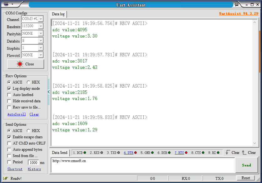
After the program is downloaded, configure the serial assistant as shown in the figure below. Adjust the potentiometer knob to output voltage to PA27 pin. When ADC collects and loads data into ADC result register 0, DMA is triggered. DMA will transfer the data to the memory variable ADC_VALUE. You can directly call ADC_VALUE to get the data.