Welcome to Wheeled Chassis Kit repository
8. ADC acquisition
ADC acquisition
ADC acquisition1. Learning objectivesADC principleADC Basic Parameters2. Hardware Construction3. Experimental steps1. Open the SYSCONFIG configuration tool2. ADC parameter configuration3. ADC acquisition channel configuration4. Write the program5. Compile4. Program Analysis5. Experimental phenomenon
1. Learning objectives
- Understand the basic knowledge of ADC.
- Learn the basic use of ADC and display the collected values on the serial assistant.
ADC principle
ADC (analog to digital converter) is an analog-to-digital converter used to convert analog signals (such as voltage) into digital signals. Analog signals change continuously, while digital signals are discrete binary numbers. ADC converts analog signals into digital data by sampling and quantizing them so that the processor or microcontroller can perform subsequent processing. According to its conversion principle, it is mainly divided into three types: successive approximation type, dual integration type, and voltage-frequency conversion type.
MSPM0G3507 uses a successive approximation (SAR) ADC, which is a common ADC working principle. The basic idea is to gradually approximate the digital representation of the input signal by comparing the magnitude relationship between the analog signal and the reference voltage. In a successive approximation ADC, the input signal and the reference voltage are compared through a differential amplifier to generate a differential voltage. This differential voltage is then input into a progressively approximated digital quantizer, which progressively compares it to a series of reference voltages. At each approximation stage, the quantizer compares the input signal to an intermediate voltage point and selects a higher or lower reference voltage as the reference for the next approximation stage based on the comparison result. This process continues until the quantizer finally approximates a digital output value.
ADC Basic Parameters
- Resolution:
- Resolution indicates the accuracy of the ADC converter output, usually measured in bits, such as 8 bits, 10 bits, 12 bits, etc. The higher the resolution, the more discrete digital values the ADC can represent, providing higher accuracy.
- MSPM0G3507 supports 8-bit, 10-bit, and 12-bit resolutions, and users can select the appropriate resolution for configuration as needed.
- Sampling Rate:
- Sampling rate (also called conversion rate) indicates the rate at which the ADC samples the analog input signal, usually expressed in samples per second (SPS). It indicates how many times the ADC can perform analog-to-digital conversions per second.
- The sampling rate of MSPM0G3507 is 4Msps (4 million samples per second), which is suitable for high-frequency signal acquisition and real-time data processing.
- Voltage reference:
- The voltage reference of the ADC is a reference voltage, which is used to compare with the analog input signal and ultimately realize the conversion of analog signals to digital signals. The accuracy and stability of the voltage reference are crucial to the conversion accuracy of the ADC.
- MSPM0G3507
supports three voltage reference configurations:
- Internal configurable reference voltage: dedicated ADC reference voltage (VREF) of 1.4V and 2.5V.
- MCU power supply voltage (VDD) is used as the reference voltage.
- External reference voltage is provided through VREF+ and VREF- pins. If the voltage reference is not configured, the MCU power supply voltage (VDD) is used as the reference voltage by default.
- Sampling range:
- The sampling range indicates the voltage range of the analog input signal that the ADC can collect, which is usually closely related to the setting of the reference voltage. The range is as follows: VREF- ≤ ADC ≤ VREF+
- VREF-: The negative end of the reference voltage, usually 0V.
- VREF+: The positive end of the reference voltage, determined by the software configuration.
These parameters together determine the performance of the ADC, including its accuracy, response speed and input voltage range.
2. Hardware Construction
MSPM0G3507 uses a successive approximation 12-bit ADC, which has 17 multiplexed channels for conversion. The 17 external channels all correspond to a pin of the microcontroller. This pin is not fixed. For details, please refer to the pin diagram or data sheet.

The A/D conversion of various channels can be configured into single, sequence conversion mode.
Single conversion mode: After each ADC conversion, the ADC will automatically stop and store the result in the ADC data register.
Repeated single conversion mode: When the ADC completes a conversion, it will automatically start another conversion and continue to convert until the continuous conversion is stopped by an external trigger or software trigger.
Multi-channel sequential single conversion mode: Used to convert multiple input channels in sequence. In this mode, the ADC will sample and convert multiple channels once according to the configured channel acquisition sequence.
Multi-channel sequential repeated conversion mode: Used to repeatedly convert multiple input channels in sequence. In this mode, the ADC will repeatedly sample and convert multiple channels according to the configured channel acquisition sequence.
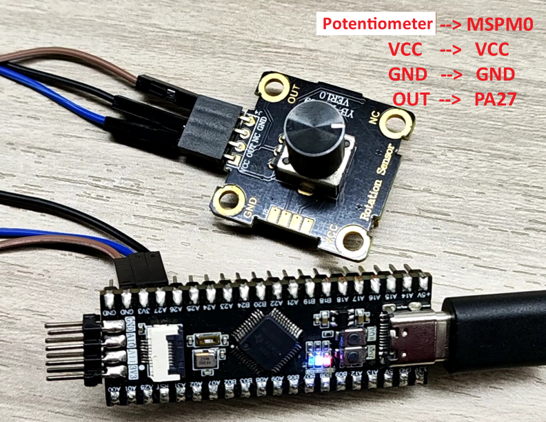
In this case, the voltage of the PA27 pin is collected by the ADC. The potentiometer module and DuPont line used in the ADC acquisition experiment need to be purchased separately, and other input voltage methods can also be used.
3. Experimental steps
This case will use the voltage of the PA27 pin as an experimental case. The voltage change is collected through ADC to print the voltage status on the serial port.
1. Open the SYSCONFIG configuration tool
Open the blank project empty in SDK in KEIL.
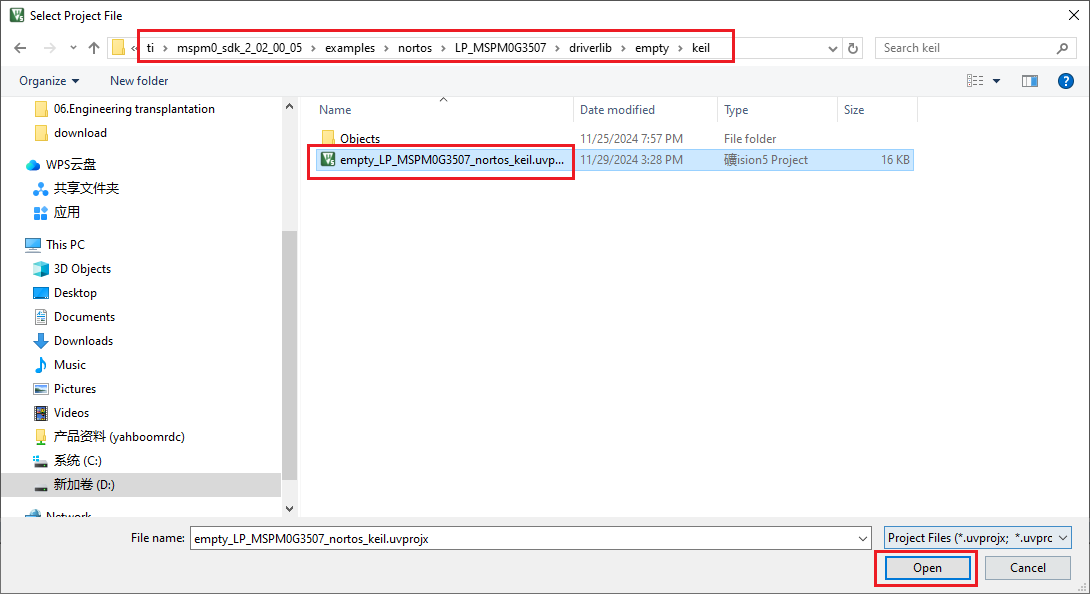
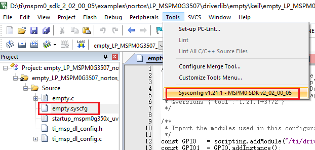
Select and open, open the empty.syscfg file in the keil interface, with the empty.syscfg file open, then select to open the SYSCONFIG GUI interface in the Tools bar.
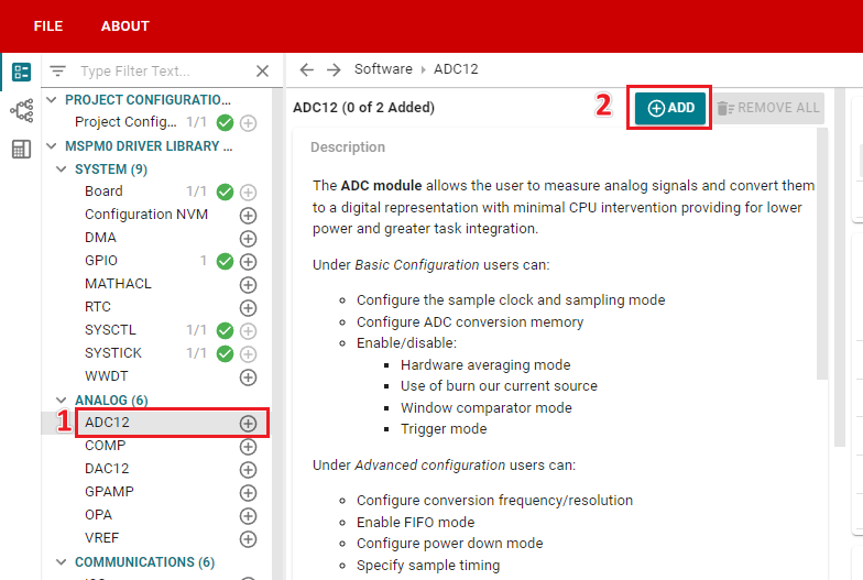
In SYSCONFIG, select MCU peripherals on the left, find the ADC12 option and click to enter. Click ADD in ADC12 to add the ADC peripheral.
2. ADC parameter configuration
The configuration of the serial port part refers to the Serial Port Communication course, which will not be described here.
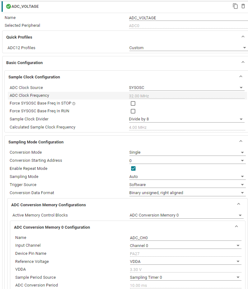
The configuration selected here is to use 32Mhz ADC frequency, 4MHz sampling frequency, single repetitive conversion mode, trigger ADC to start sampling through software, and the data format is binary right-aligned.
Parameter Description:
ADC Clock Source: ADC clock source. Set to SYSOSC(32MHz).
ADC Clock Frequency: Displays the current ADC clock frequency.
Sample Clock Divider: Sampling divider. Configured as 8 dividers.
Calculated Sample clock Freguency: Displays the sampling frequency after frequency division.
Conversion Mode: Conversion mode. Configured as Single, single shot.
Conversion Starting Address: Conversion starting address. Configure to start sampling from the 0th (related to the storage register behind).
Enable Repeat Mode: Whether to enable repeated conversion. Check here to enable.
Sampling Mode: Sampling mode. Set to Auto, automatic.
Trigger Source: ADC trigger mode. Configured as Software software trigger mode.
Conversion Data Format: ADC data conversion format. Configured as Binary unsigned, right aligned binary format right alignment mode.
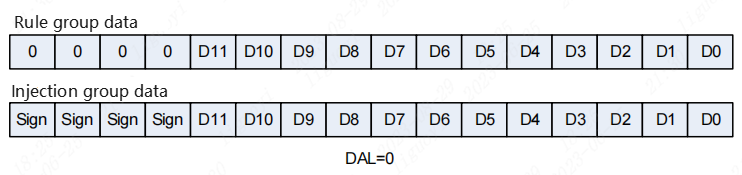
The ADC of MSPM0G3507 supports multiple data alignment methods to adapt to different application scenarios. Common data alignment methods include left alignment and right alignment.
- Right alignment mode: In right alignment mode, the ADC data is right-aligned to the lowest bit after the conversion, and the insufficient bits are filled with 0 in the high bit. Right-aligned mode allows for better dynamic range without loss of precision.
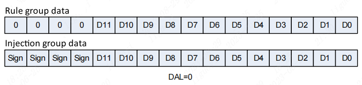
- Left-aligned mode: In left-aligned mode, the ADC data is left-aligned to the highest bit, and the insufficient bits are filled with 0 in the lower bit. Left-aligned mode can improve resolution, but will result in a reduced dynamic range.
We configure it to right-aligned so that we can directly operate on the converted data.
3. ADC acquisition channel configuration
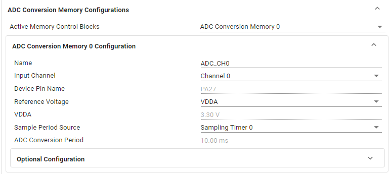
Parameter description:
Active Memory Control Blocks: ADC data storage address. Store ADC conversion results in register 0.
Input Channel: Input channel. Select channel 0 (each channel corresponds to a different pin).
Device Pin Name: Pin automatically selected according to the channel, the pin of channel 0 is PA27.
Reference Voltage: Voltage reference. Configured to use MCU power supply VDDA.
ADC Conversion Period: Displays the time it takes for the ADC to convert a single data.
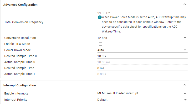
Parameter Description:
Conversion Resolution: The resolution is configured to 12-bits.
Desired Sample Time 0: The sampling time is set to 10ms.
Enable interrupts: Enable the interrupt for ADC acquisition completion. When the ADC acquisition is completed, the interrupt is triggered and we process the data.

Click SAVE to save the configuration in SYSCONFIG, then turn off SYSCONFIG and return to keil.
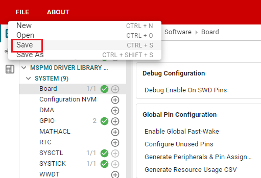
Select Yes to All in the pop-up window
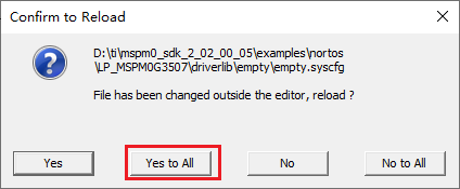
Similarly, we also need to confirm whether the ti_msp_dl_config.c and ti_msp_dl_config.h files are updated. Compile directly, and the compilation will automatically update to keil. If there is no update, we can also copy the file content in SYSCONFIG.
4. Write the program
In the empty.c file, write the following code
x#include "ti_msp_dl_config.h"#include "stdio.h"volatile unsigned int delay_times = 0;volatile bool gCheckADC; //ADC采集成功标志位 ADC acquisition success flagvoid delay_ms(unsigned int ms); //搭配滴答定时器的精准毫秒级延时 Precise millisecond delay with tick timerunsigned int adc_getValue(void);//读取ADC的数据 Read ADC data/******************************串口重定向 Serial port redirection***************************************/#if !defined(__MICROLIB)//不使用微库的话就需要添加下面的函数//If you don't use the micro library, you need to add the following function#if (__ARMCLIB_VERSION <= 6000000)//如果编译器是AC5 就定义下面这个结构体//If the compiler is AC5, define the following structurestruct __FILE{ int handle;};#endifFILE __stdout;//定义_sys_exit()以避免使用半主机模式// define _sys_exit() to avoid using semihost modevoid _sys_exit(int x){ x = x;}#endif//printf函数重定义 printf function redefinitionint fputc(int ch, FILE *stream){ //当串口0忙的时候等待,不忙的时候再发送传进来的字符 // Wait when serial port 0 is busy, and send the incoming characters when it is not busy while( DL_UART_isBusy(UART_0_INST) == true ); DL_UART_Main_transmitData(UART_0_INST, ch); return ch;}/*********************************************************************/int main(void){ unsigned int adc_value = 0; unsigned int voltage_value = 0; SYSCFG_DL_init(); //清除串口中断标志 Clear the serial port interrupt flag NVIC_ClearPendingIRQ(UART_0_INST_INT_IRQN); //开启串口中断 Enable serial port interrupt NVIC_EnableIRQ(UART_0_INST_INT_IRQN); //开启ADC中断 Enable ADC interrupt NVIC_EnableIRQ(ADC_VOLTAGE_INST_INT_IRQN); printf("adc Demo start\r\n"); while (1) { //获取ADC数据 Get ADC data adc_value = adc_getValue(); printf("adc value:%d\r\n", adc_value); //将ADC采集的数据换算为电压 Convert the data collected by ADC into voltage voltage_value = (int)((adc_value/4095.0*3.3)*100); printf("voltage value:%d.%d%d\r\n", voltage_value/100, voltage_value/10%10, voltage_value%10 ); delay_ms(1000); }}//延时函数 Delay functionvoid delay_ms(unsigned int ms){ delay_times = ms; while( delay_times != 0 );}//读取ADC的数据 Read ADC dataunsigned int adc_getValue(void){ unsigned int gAdcResult = 0; //软件触发ADC开始转换 Software triggers ADC to start conversion DL_ADC12_startConversion(ADC_VOLTAGE_INST); //如果当前状态为正在转换中则等待转换结束 // If the current state is converting, wait for the conversion to end while (false == gCheckADC) { __WFE(); } //获取数据 Get data gAdcResult = DL_ADC12_getMemResult(ADC_VOLTAGE_INST, ADC_VOLTAGE_ADCMEM_ADC_CH0); //清除标志位 Clear flag gCheckADC = false; return gAdcResult;}//滴答定时器的中断服务函数 Tick ??timer interrupt service functionvoid SysTick_Handler(void){ if( delay_times != 0 ) { delay_times--; }}//ADC中断服务函数 ADC interrupt service functionvoid ADC_VOLTAGE_INST_IRQHandler(void){ //查询并清除ADC中断 Query and clear ADC interrupt switch (DL_ADC12_getPendingInterrupt(ADC_VOLTAGE_INST)) { //检查是否完成数据采集 Check whether data collection is completed case DL_ADC12_IIDX_MEM0_RESULT_LOADED: gCheckADC = true;//将标志位置1 Set the flag position to 1 break; default: break; }}5. Compile
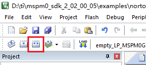
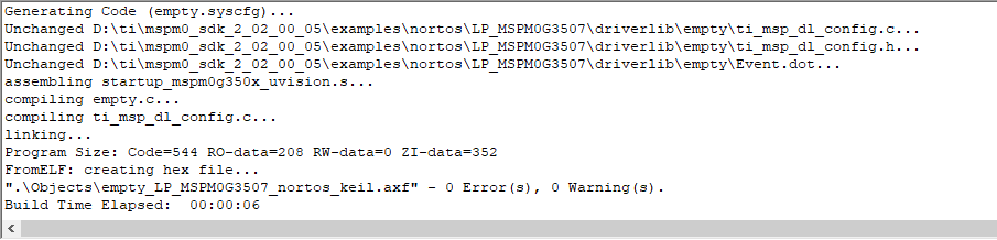
Click the Rebuild icon. The following prompt appears, indicating that the compilation is complete and there are no errors.
4. Program Analysis
- empty.c
xxxxxxxxxx//读取ADC的数据 Read ADC dataunsigned int adc_getValue(void){ unsigned int gAdcResult = 0; //软件触发ADC开始转换 Software triggers ADC to start conversion DL_ADC12_startConversion(ADC_VOLTAGE_INST); //如果当前状态为正在转换中则等待转换结束 // If the current state is converting, wait for the conversion to end while (false == gCheckADC) { __WFE(); } //获取数据 Get data gAdcResult = DL_ADC12_getMemResult(ADC_VOLTAGE_INST, ADC_VOLTAGE_ADCMEM_ADC_CH0); //清除标志位 Clear flag gCheckADC = false; return gAdcResult;}Call the DL_ADC12_startConversion function to start ADC conversion. If the current ADC is still converting, the program enters low power mode through __WFE() until the interrupt sets the gCheckADC flag, indicating that the conversion is complete. After the conversion is completed, call DL_ADC12_getMemResult to get the conversion result and return
xxxxxxxxxx//滴答定时器的中断服务函数 Tick ??timer interrupt service functionvoid SysTick_Handler(void){ if( delay_times != 0 ) { delay_times--; }}//ADC中断服务函数 ADC interrupt service functionvoid ADC_VOLTAGE_INST_IRQHandler(void){ //查询并清除ADC中断 Query and clear ADC interrupt switch (DL_ADC12_getPendingInterrupt(ADC_VOLTAGE_INST)) { //检查是否完成数据采集 Check whether data collection is completed case DL_ADC12_IIDX_MEM0_RESULT_LOADED: gCheckADC = true;//将标志位置1 Set the flag position to 1 break; default: break; }}SysTick_Handler: tick timer interrupt service function, used to implement delay. Each time an interrupt occurs, delay_times is reduced by 1 until it reaches 0 to stop the delay.
ADC_VOLTAGE_INST_IRQHandler: ADC interrupt service function. When the ADC conversion is completed, check the ADC interrupt and set the flag gCheckADC to inform the main program that data can be read.
xxxxxxxxxxint main(void){ unsigned int adc_value = 0; unsigned int voltage_value = 0; SYSCFG_DL_init(); //清除串口中断标志 Clear the serial port interrupt flag NVIC_ClearPendingIRQ(UART_0_INST_INT_IRQN); //开启串口中断 Enable serial port interrupt NVIC_EnableIRQ(UART_0_INST_INT_IRQN); //开启ADC中断 Enable ADC interrupt NVIC_EnableIRQ(ADC_VOLTAGE_INST_INT_IRQN); printf("adc Demo start\r\n"); while (1) { //获取ADC数据 Get ADC data adc_value = adc_getValue(); printf("adc value:%d\r\n", adc_value); //将ADC采集的数据换算为电压 Convert the data collected by ADC into voltage voltage_value = (int)((adc_value/4095.0*3.3)*100); printf("voltage value:%d.%d%d\r\n", voltage_value/100, voltage_value/10%10, voltage_value%10 ); delay_ms(1000); }}After initializing the system configuration, enable the interrupts of the serial port and ADC. In the main loop, call adc_getValue() to get the ADC data, convert it into a voltage value and print it.
5. Experimental phenomenon
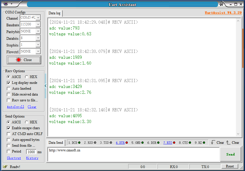
After the program is downloaded, configure the serial port assistant as shown below, adjust the potentiometer knob, and you can see the effect of the real-time change of voltage between 0-3.3v in the serial port assistant receiving window.