Welcome to Self-balancing Robot Car repository
02.LED Control(GPIO)
LED Control
LED ControlHardware connectionControl principleBit-band operationAdvantagesCodeExampleSoftware configurationPin definitionSoftware codecontrol functionExperimental phenomenon
The tutorial demonstrates controlling the LED on and off.
The tutorial only introduces the standard library project code
Hardware connection
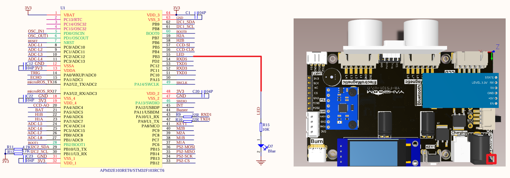
| Peripherals | Development Board | Description |
|---|---|---|
| LED | PB3 | The anode of the LED is connected to the development board PB3, and the cathode is connected to the development board GND |
Control principle
By controlling the PB3 pin to output high and low levels, the LED can be turned on and off.
| Control pin | Output level | LED effect |
|---|---|---|
| PB3 | Output low level | LED off |
| PB3 | Output high level | LED on |
Bit-band operation
xxxxxxxxxxFor specific implementation ideas, refer to Chapter 5 (pages 87 to 92) of <<CM3 Authoritative Guide>>
Using bit-band operation, you can read and write a single bit of the memory.
Bit-band area: address area supporting bit-band operation
Bit-band alias: access to alias address ultimately affects access to bit-band area
Range of two memory areas supporting bit-band operation
SRAM bit-band area address: 0x2000 0000 - 0x200F FFFF
Peripheral bit-band area address: 0x4000 0000 - 0x400F FFFF
Bit-band alias area
A: byte address
n: bit number (0≤n≤7)
SRAM bit-band alias area address: 0x2200 0000 - 0x23FF FFFC
xxxxxxxxxxAliasAddr= =0x22000000+ ((A-0x20000000)*8 +n)*4
Peripheral bit-band alias area address: 0x4200 0000 - 0x43FF FFFC
xxxxxxxxxxAliasAddr= =0x42000000+ ((A-0x40000000)*8 +n)*4
Advantages
You can directly control the bits of the hardware register to improve program execution efficiency!
Code
x// A macro that converts "bit with address + bit serial number" to an alias address#define BITBAND(addr, bitnum) ((addr & 0xF0000000)+0x2000000+((addr &0xFFFFF)<<5)+(bitnum<<2))// Converts an address to a pointer#define MEM_ADDR(addr) *((volatile unsigned long *)(addr))// Converts the bit-tape alias area address to a pointer#define BIT_ADDR(addr, bitnum) MEM_ADDR(BITBAND(addr, bitnum))// GPIO ODR and IDR register address mapping#define GPIOA_ODR_Addr (GPIOA_BASE+12) //0x4001080C#define GPIOB_ODR_Addr (GPIOB_BASE+12) //0x40010C0C#define GPIOC_ODR_Addr (GPIOC_BASE+12) //0x4001100C#define GPIOD_ODR_Addr (GPIOD_BASE+12) //0x4001140C#define GPIOE_ODR_Addr (GPIOE_BASE+12) //0x4001180C#define GPIOF_ODR_Addr (GPIOF_BASE+12) //0x40011A0C#define GPIOG_ODR_Addr (GPIOG_BASE+12) //0x40011E0C#define GPIOA_IDR_Addr (GPIOA_BASE+8) //0x40010808#define GPIOB_IDR_Addr (GPIOB_BASE+8) //0x40010C08#define GPIOC_IDR_Addr (GPIOC_BASE+8) //0x40011008#define GPIOD_IDR_Addr (GPIOD_BASE+8) //0x40011408#define GPIOE_IDR_Addr (GPIOE_BASE+8) //0x40011808#define GPIOF_IDR_Addr (GPIOF_BASE+8) //0x40011A08#define GPIOG_IDR_Addr (GPIOG_BASE+8) //0x40011E08// Operate an I/O port of GPIO alone, n(0,1,2...) 15),n indicates the specific I/O port#define PAout(n) BIT_ADDR(GPIOA_ODR_Addr,n) // Output#define PAin(n) BIT_ADDR(GPIOA_IDR_Addr,n) // Enter#define PBout(n) BIT_ADDR(GPIOB_ODR_Addr,n) // Output#define PBin(n) BIT_ADDR(GPIOB_IDR_Addr,n) // Input#define PCout(n) BIT_ADDR(GPIOC_ODR_Addr,n) // Outputdefine PCin(n) BIT_ADDR(GPIOC_IDR_Addr,n) // Enter#define PDout(n) BIT_ADDR(GPIOD_ODR_Addr,n) // Output#define PDin(n) BIT_ADDR(GPIOD_IDR_Addr,n) // Enter this parameter#define PEout(n) BIT_ADDR(GPIOE_ODR_Addr,n) // Output#define PEin(n) BIT_ADDR(GPIOE_IDR_Addr,n) // Enter a value#define PFout(n) BIT_ADDR(GPIOF_ODR_Addr,n) // Output#define PFin(n) BIT_ADDR(GPIOF_IDR_Addr,n) // Enter#define PGout(n) BIT_ADDR(GPIOG_ODR_Addr,n) // Output#define PGin(n) BIT_ADDR(GPIOG_IDR_Addr,n) // Input
Example
PB3 output low
The following code actually works the same, the bitband operation is relatively simpler and faster!
Standard Library
xxxxxxxxxxGPIO_ResetBits(GPIOB,GPIO_Pin_3)GPIO_WriteBit(GPIOB, GPIO_Pin_3, Bit_RESET)
Bit band operation
xxxxxxxxxxPBout(3) = 0;
Software configuration
Pin definition
| pin of the main control chip | main function (after reset) | default reuse function | redefine function | |
|---|---|---|---|---|
| STM32F103RCT6 | PB3 | JTDO | SPI3_SCK/I2S3_CK | PB3/TRACESWO TIM2_CH2/ SPI1_SCK |
Software code
Since the default function of the PB3 pin is the JTDO function, we need to disable its function and configure the PB3 as a normal IO pin function.
xxxxxxxxxxProduct supporting information source path: attachment → source summary → 1.Base_Course → 2.LED
control function
The tutorial only briefly introduces the code, the specific can open the project source code to read.
Init_Led_GPIO
xxxxxxxxxxvoid Init_Led_GPIO(void){GPIO_InitTypeDef GPIO_InitStructure;RCC_APB2PeriphClockCmd(LED_RCC, ENABLE);GPIO_InitStructure.GPIO_Pin = LED_PIN;GPIO_InitStructure.GPIO_Mode = GPIO_Mode_Out_PP;GPIO_InitStructure.GPIO_Speed = GPIO_Speed_2MHz;GPIO_Init(LED_PORT, &GPIO_InitStructure);LED = 0;}
Experimental phenomenon
The LEd.hex file generated by the project compilation is located in the OBJ folder of the LED project, find the corresponding LEd.hex file of the project and use FlyMcu software to download the program into the development board.
After the program is successfully downloaded, the LED switches on and off every 500ms.