Welcome to MSPM0 Smart Robot Car repository
6. Temperature Detection (ADC)
Temperature Detection
Temperature DetectionI. Learning ObjectivesII. Hardware SetupIII. Experiment StepsIV. Program AnalysisV. Experiment Phenomenon
I. Learning Objectives
- Understand basic ADC knowledge.
- Learn basic ADC usage, printing collected internal temperature values through serial port.
ADC Principle
ADC (analog to digital converter) is an analog-to-digital converter used to convert analog signals (such as voltage) into digital signals. Analog signals change continuously, while digital signals are discrete binary numbers. ADC converts analog signals into digital data through sampling and quantization, so that processors or microcontrollers can perform subsequent processing. According to their conversion principles, they are mainly divided into three types: successive approximation type, dual-slope integration type, and voltage-frequency conversion type.
MSPM0G3507 uses a successive approximation (SAR) ADC, which is a common ADC working principle. Its basic idea is to gradually approximate the digital representation of the input signal by comparing the magnitude relationship between the analog signal and the reference voltage. In successive approximation ADCs, the input signal and reference voltage are compared through a differential amplifier to produce a differential voltage. Then, this differential voltage is input to a successive approximation digital quantizer, which gradually compares it with a series of reference voltages. At each approximation stage, the quantizer compares the input signal with an intermediate voltage point and selects a higher or lower reference voltage as the reference for the next approximation stage based on the comparison result. This process continues until the quantizer finally approximates to a digital output value.
ADC Basic Parameters
Resolution:
- Resolution represents the precision of the ADC converter output, usually measured in bits, such as 8-bit, 10-bit, 12-bit, etc. The higher the resolution, the more discrete digital values the ADC can represent, thereby providing higher precision.
Sampling Rate:
- Sampling rate (also called conversion rate) represents the rate at which the ADC samples the analog input signal, usually expressed in samples per second (SPS). It indicates how many analog-to-digital conversions the ADC can perform per second.
- MSPM0G3507 has a sampling rate of 4Msps (4 million samples per second), suitable for high-frequency signal acquisition and real-time data processing.
Voltage Reference:
The ADC voltage reference is a reference voltage used to compare with the analog input signal to ultimately achieve analog-to-digital signal conversion. The accuracy and stability of the voltage reference are crucial to the ADC conversion precision.
MSPM0G3507
supports three voltage reference configurations:
- Internal configurable reference voltage: 1.4V and 2.5V dedicated ADC reference voltage (VREF).
- MCU power supply voltage (VDD) as reference voltage.
- External reference voltage provided through VREF+ and VREF- pins. If no voltage reference is configured, the MCU's power supply voltage (VDD) is used as the reference voltage by default.
Sampling Range:
Sampling range represents the voltage range of analog input signals that the ADC can collect, usually closely related to the reference voltage setting. The range is as follows: VREF- ≤ ADC ≤ VREF+
- VREF-: Set reference voltage negative terminal, usually 0V.
- VREF+: Set reference voltage positive terminal, determined according to software configuration.
These parameters together determine the ADC performance, including its precision, response speed, and input voltage range.
II. Hardware Setup
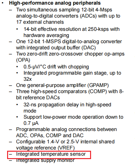
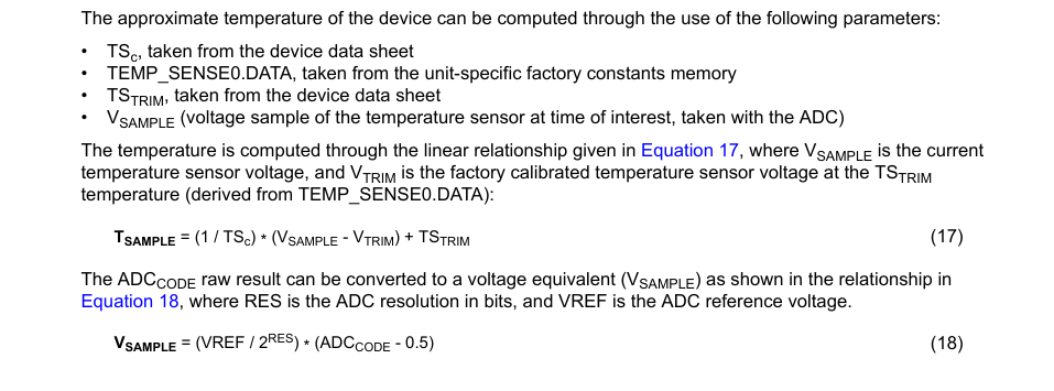
The data sheet feature description states that MSPM0 has an integrated temperature sensor that can roughly feedback chip temperature
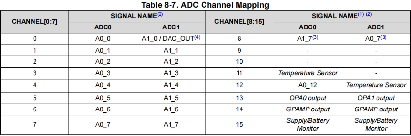
The temperature sensor is internally connected to ADC channel 11 and channel 12. Here we take ADC0 peripheral conversion channel 11 as an example
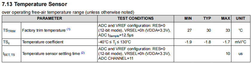
The following is the data sheet description of the temperature sensor
A unit-specific single-point trim value (TEMP_SENSE0.DATA) is provided in each device's factory constant memory. This value represents the output voltage of the temperature sensor at the factory temperature (TSTRIM), expressed in ADC result code format. The ADC result code in TEMP_SENSE0. Data is based on 12-bit sampling mode, and the temperature sensor outputs a voltage linearly related to temperature. The temperature coefficient (TSc) is the slope of the temperature-voltage relationship (in mV/C), given in the specifications section of the device-specific data sheet (as shown in the table below)
III. Experiment Steps
Import Project
In KEIL, open our serial communication project from the previous section, or you can use the project template from the 80MHz clock frequency configuration chapter or the empty project from the SDK.
After selecting and opening, in the KEIL interface, open the empty.syscfg file. With the empty.syscfg file open, select Open SYSCONFIG GUI interface from the Tools menu.
Add ADC Peripheral Configuration
The source code for this tutorial is based on the source code from tutorial 4 Serial Communication.
In SYSCONFIG, select MCU peripherals on the left, find ADC12 option and click to enter. In ADC12, click ADD to add ADC peripheral. Here we name it Temperature
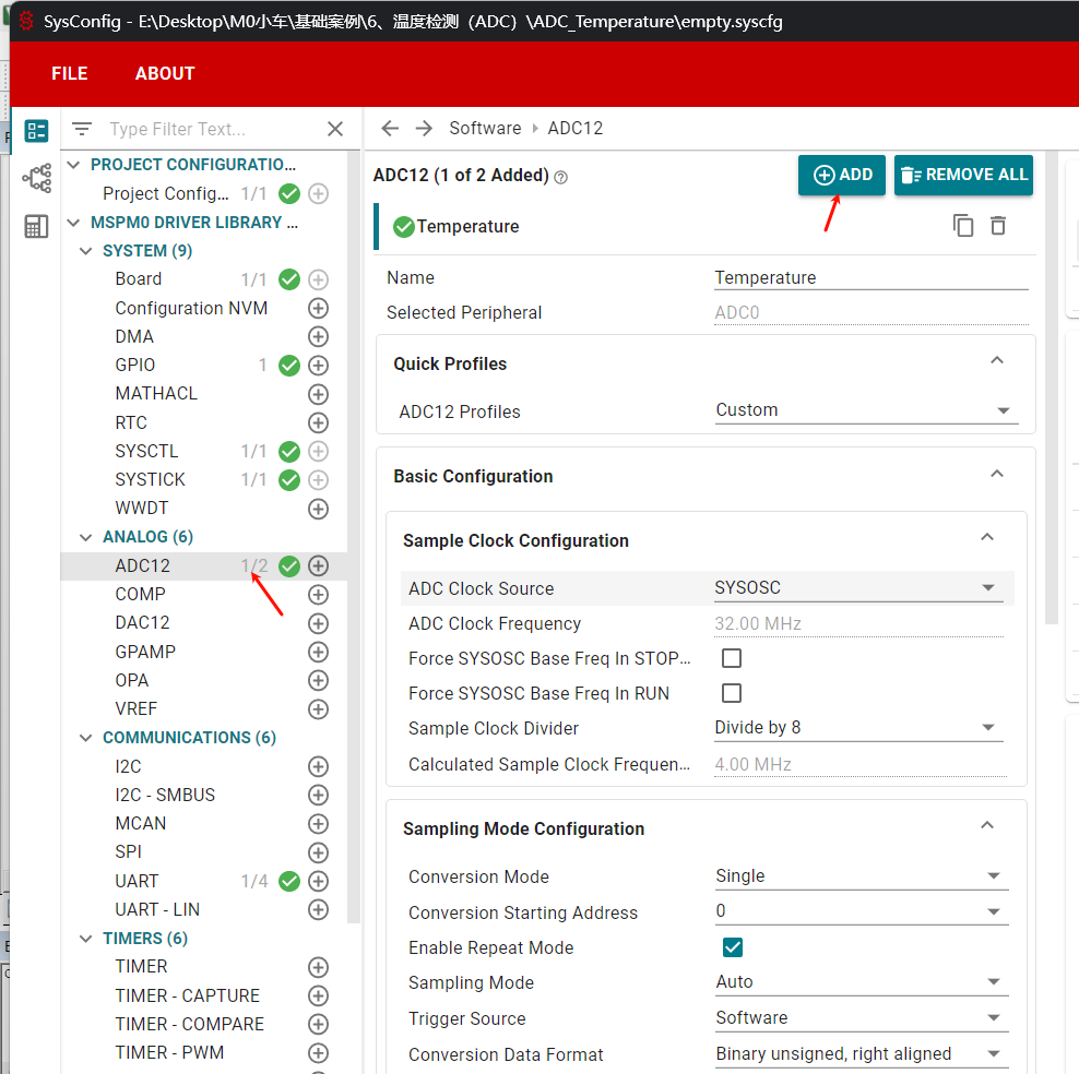
The configuration selected here is to use 32MHz ADC frequency, sampling frequency of 4MHz, single repeat conversion mode, ADC sampling is triggered by software, data format is binary right-aligned. We set the sampling time to 10ms
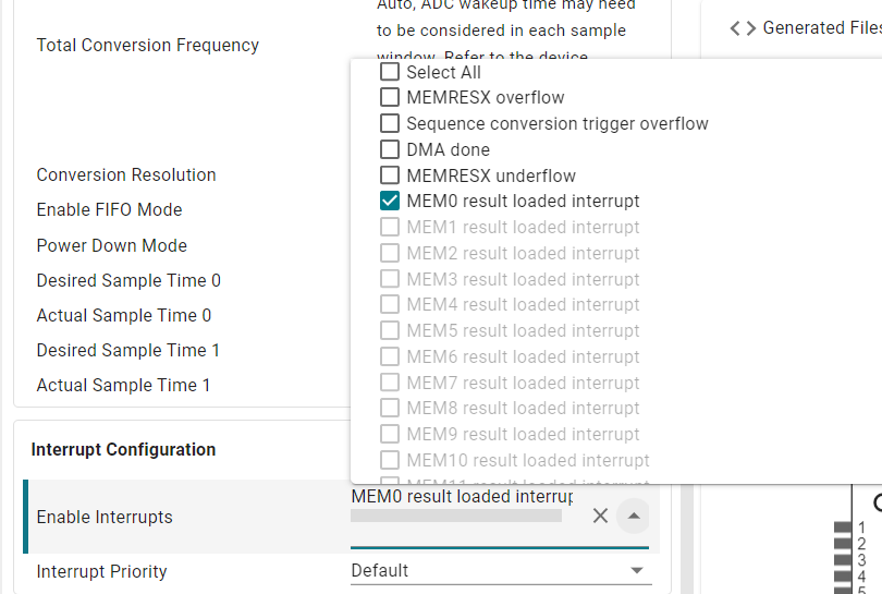
Enable channel 0 result load interrupt
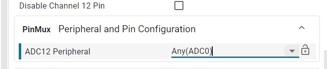
Configure as ADC0 as conversion peripheral
Parameter description:
ADC Clock Source: ADC clock source. Set to SYSOSC(32MHz).
ADC Clock Frequency: Shows the current ADC clock frequency.
Sample Clock Divider: Sampling divider. Configured as divide by 8.
Calculated Sample clock Frequency: Shows the sampling frequency after division.
Conversion Mode: Conversion mode. Configured as Single, single.
Conversion Starting Address: Conversion start address. Configured to start sampling from the 0th (related to the storage register below).
Enable Repeat Mode: Whether to enable repeat conversion. Checked here, enabled.
Sampling Mode: Sampling method. Set to Auto, automatic.
Trigger Source: ADC trigger method. Configured as Software software trigger method.
Conversion Data Format: ADC data conversion format. Configured as Binary unsigned, right aligned binary format right-aligned method.
MSPM0G3507's ADC supports multiple data alignment methods to adapt to different application scenarios. Common data alignment methods include left-aligned and right-aligned.
- Right-aligned mode: In right-aligned mode, the ADC data is right-aligned to the least significant bits after conversion, with insufficient bits filled with 0 in the high bits. Right-aligned mode allows for better dynamic range without precision loss.
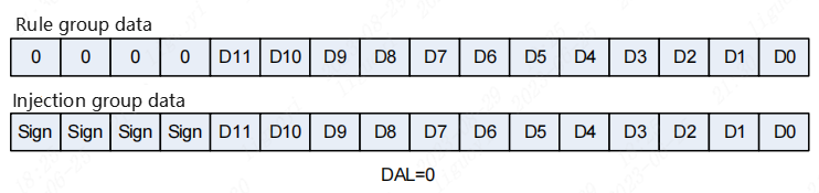
- Left-aligned mode: In left-aligned mode, the ADC data is left-aligned to the most significant bits, with insufficient bits filled with 0 in the low bits. Left-aligned mode can improve resolution but results in reduced dynamic range.
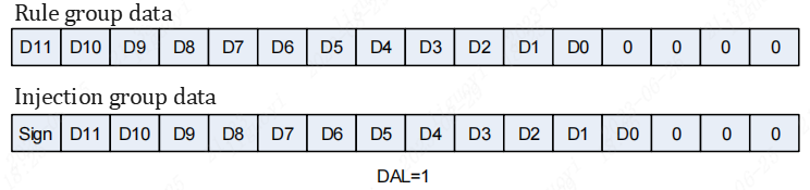
We configure as right-aligned method, so we can directly perform calculations on the converted data.
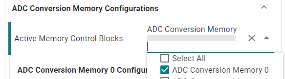
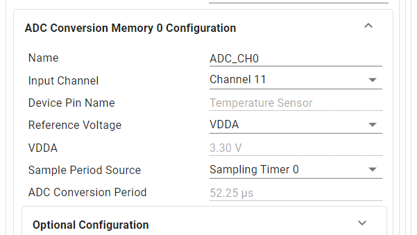
ADC conversion channel configuration puts conversion results in memory 0
Parameter description:
Active Memory Control Blocks: ADC data storage address. Store ADC conversion result in register 0.
Input Channel: Input channel. Select channel 0 (each channel corresponds to different pins).
Device Pin Name: Pin automatically selected according to channel, channel 0 pin is PA27.
Reference Voltage: Voltage reference. Configured to use MCU power supply VDDA.
ADC Conversion Period: Shows the time for ADC to convert a single data
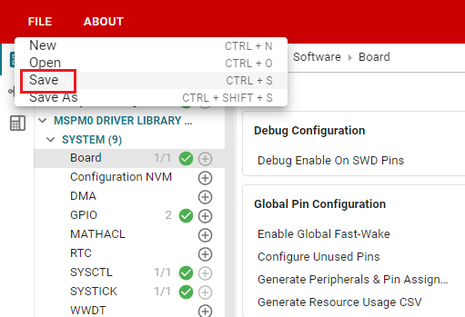
Click SAVE to save the configuration in SYSCONFIG, then close SYSCONFIG and return to keil.
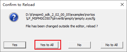
Select Yes to All in the pop-up window
IV. Program Analysis
Like the previous section, we create new bsp_vol_adc.c, bsp_vol_adc.h under the BSP file, configured as follows
temperature_adc.h
xxxxxxxxxx//extern volatile bool gCheckADC;extern volatile float gTemperatureDegC;extern volatile float gTemperatureDegF;temperature_adc.c
xxxxxxxxxxvolatile bool gCheckADC;volatile float gTemperatureDegC;volatile float gTemperatureDegF;/** * @brief Temperature ADC interrupt service routine * @brief 温度ADC中断服务函数 */void Temperature_INST_IRQHandler(void){ //Check and process ADC interrupt sources //检查并处理ADC中断源 switch (DL_ADC12_getPendingInterrupt(Temperature_INST)) { //ADC MEM0 result loaded interrupt //ADC MEM0结果加载中断 case DL_ADC12_IIDX_MEM0_RESULT_LOADED: //Set ADC completion flag //设置ADC完成标志位 gCheckADC = true; break; //Other interrupt cases //其他中断情况 default: break; }}empty.c
xxxxxxxxxxint main(void){ //ADC sampling result / ADC采样结果 uint32_t adcResult; //tempDegC: Celsius temperature / 摄氏温度 //tempDegF: Fahrenheit temperature / 华氏温度 //vSample: Current voltage / 当前电压 //vTrim: Output voltage of temperature sensor at factory calibration temperature TEMP_TS_TRIM_C float vSample, vTrim, tempDegC, tempDegF; //System configuration initialization SYSCFG_DL_init(); //Get factory calibration value and convert to voltage //DL_SYSCTL_getTempCalibrationConstant reads ADC value from TEMP_SENSE0.DATA vTrim = (DL_SYSCTL_getTempCalibrationConstant() - 0.5f) * ADC_VREF_VOLTAGE / ADC_BIT_RESOLUTION; //Enable temperature ADC interrupt NVIC_EnableIRQ(Temperature_INST_INT_IRQN); gCheckADC = false; while (1) { //Start ADC conversion DL_ADC12_startConversion(Temperature_INST); //Wait for conversion to complete while (false == gCheckADC) { __WFE(); } gCheckADC = false; //Stop ADC conversion DL_ADC12_stopConversion(Temperature_INST); //Collect ADC value of current temperature adcResult = DL_ADC12_getMemResult(Temperature_INST, Temperature_ADCMEM_ADC_CH0); //Convert ADC result to voltage value vSample = (adcResult - 0.5f) * ADC_VREF_VOLTAGE / ADC_BIT_RESOLUTION; //Calculate temperature (Celsius) //Formula: Temp = (V_sample - V_trim) * Coeff + Trim_Temp tempDegC = (vSample - vTrim) * TEMP_TS_COEF_mV_C * 1000.0f + TEMP_TS_TRIM_C; //Note: Coefficient TEMP_TS_COEF_mV_C comes from data sheet //Multiply by 1000 above converts millivolts to volts, because vSample and vTrim units are volts (V) //Calculate Fahrenheit temperature tempDegF = tempDegC * 9.0f / 5.0f + 32.0f; //Update global temperature variables gTemperatureDegC = tempDegC; gTemperatureDegF = tempDegF; //Print temperature value (retain 1 decimal place) printf("%3.1f℃ \r\n", gTemperatureDegC); }}V. Experiment Phenomenon
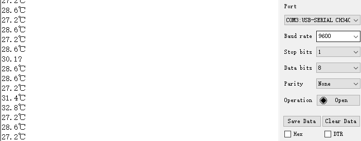
We connect Type-C to the computer and the car, then open the serial debugging assistant, baud rate 9600, eight data bits, one stop bit, no parity.
Note that when using Type-C as debugging serial port output, it is not recommended to connect other sensors to serial port 0!