Welcome to MSPM0 Smart Robot Car repository
13. Internal Flash (Flash)
On-chip Flash (Flash)
On-chip Flash (Flash)I. Learning ObjectivesII. Flash IntroductionIII. Hardware SetupIV. Software Environment SetupV. Code AnalysisVI. Experiment Phenomenon
I. Learning Objectives
- Learn and understand basic flash knowledge.
- Learn to read and write the flash of MSPM0G3507.
The DAP-LINK debugging tool used in this tutorial section needs to be prepared by yourself
II. Flash Introduction
First, we need to understand several unit terms
Sector: Sector (1KB)
BANK: A group of sectors that can be batch erased in a single operation; only one operation (read, program, erase, or verify) can run simultaneously on the same Bank, maximum 256 sectors
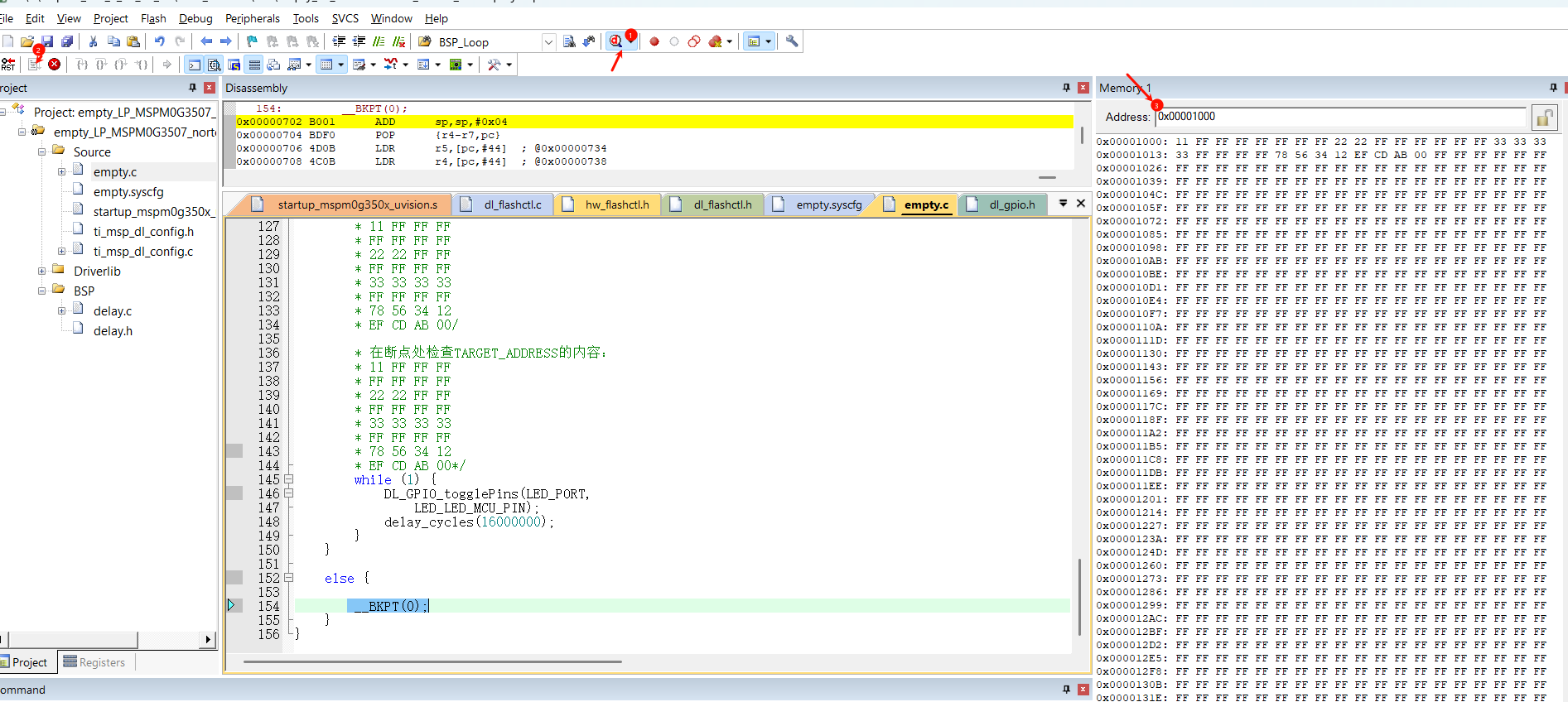
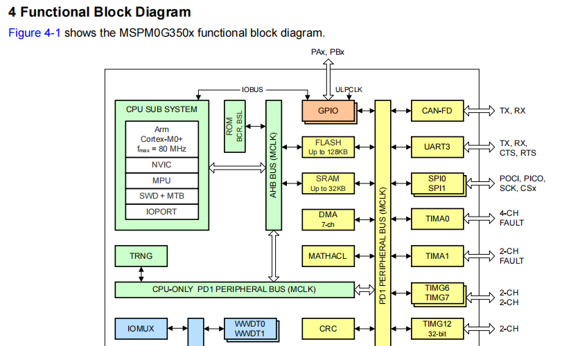
MSPM0G350x has flash memory with error correction code (ECC) and up to 128KB, where the first 32KB has 100,000 programming/erasing cycles (addresses 0x0000.0000 to 0x0000.8000), and up to 10,000 programming/erasing cycles can be performed on the remaining flash. Flash is used to store application code and data, device startup configuration, and parameters pre-programmed by TI from the factory. In this section, we will write specified data to flash starting from address 0x00001000 and then view it through simulation tools.


III. Hardware Setup
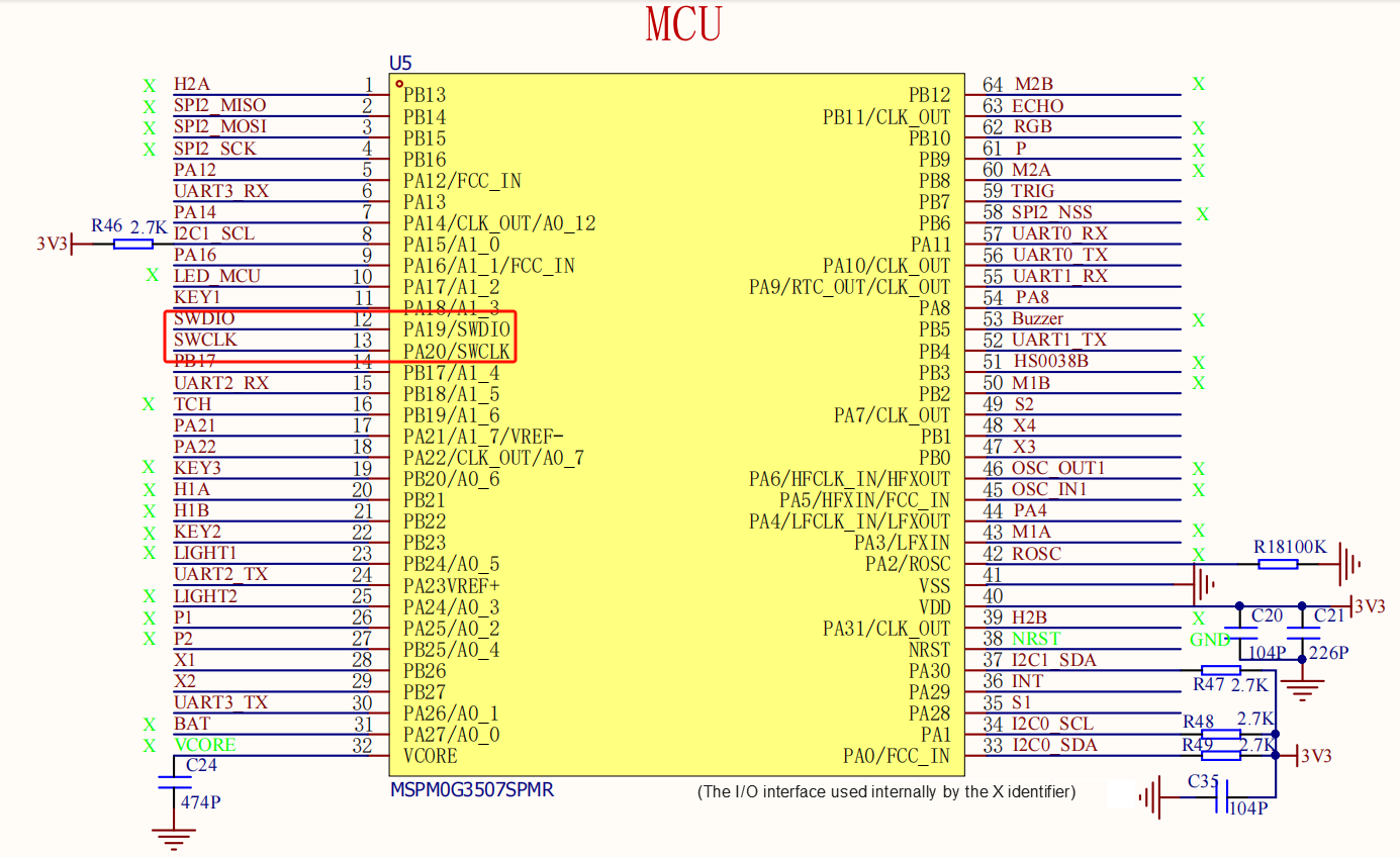
This course requires connecting a debugging tool, using DAP-Link as an example. For details, please refer to [M0 Car Development Board Instructions] SWD Debug Interface
| DAP-LINK | MSPM0G3507 |
|---|---|
| GND | GND |
| VDD or 3V3 | 3V3 |
| SWCLK/CLK | SWCLK(PA20) |
| SWDIO/DIO | SWDIO(PA19) |
IV. Software Environment Setup
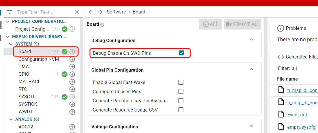
In this tutorial section, we will build based on the LED project. First, we open SWD through sysconfig, then save and generate code
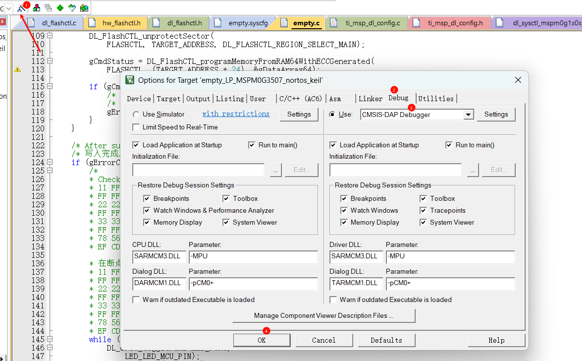
Configure the programmer, using DAP-LINK as an example here. Other programmers can be selected according to your own configuration.
V. Code Analysis
xxxxxxxxxxFlash writing process: Unprotect -> Erase Sector/Bank -> Write specified data /* Unprotect sectors in main memory (hardware generates ECC) */ DL_FlashCTL_unprotectSector( FLASHCTL, TARGET_ADDRESS, DL_FLASHCTL_REGION_SELECT_MAIN); /* Erase sectors in main memory */ gCmdStatus = DL_FlashCTL_eraseMemoryFromRAM( FLASHCTL, TARGET_ADDRESS, DL_FLASHCTL_COMMAND_SIZE_SECTOR); if (gCmdStatus == DL_FLASHCTL_COMMAND_STATUS_FAILED) { /* If command execution fails, set error flag */ gErrorCode = ERROR_ERASE; } if (gErrorCode == NO_ERROR) { /* Perform 8-bit write to main memory flash */ DL_FlashCTL_unprotectSector( FLASHCTL, TARGET_ADDRESS, DL_FLASHCTL_REGION_SELECT_MAIN); gCmdStatus = DL_FlashCTL_programMemoryFromRAM8WithECCGenerated( FLASHCTL, TARGET_ADDRESS, &gData8); if (gCmdStatus == DL_FLASHCTL_COMMAND_STATUS_FAILED) { /* If command execution fails, set error flag */ gErrorCode = ERROR_8BIT_W; } }VI. Experiment Phenomenon
After the program is flashed, write one byte, two bytes, three bytes, and four bytes of data to the specified position sequentially. After writing is completed, the MCU indicator light will flash once every 1 second. We can view the written values through debugging tools