Welcome to ESP32 Core Board repository
8. ADC
ADC
ADC1. ADC Overview2. Core Concepts2.1 ADC Conversion Principle2.2 Bit Width and Resolution2.3 Attenuation Configuration2.4 Two Driver Modes3. ESP32-S3 ADC Hardware Characteristics4. Project Architecture and Flow5. Hardware Dependencies6. Source Code Analysis6.1 Header Files and Macro Configuration6.2 adc_init() — Initialization6.3 adc_read_loop() — Acquisition Loop6.4 app_main() — Main Entry7. Operation Flow7.1 Build and Flash7.2 Normal Acquisition7.2 Boundary Cases8. Common Issues
1. ADC Overview
ADC (Analog-to-Digital Converter) converts continuously varying analog voltage (from potentiometers, sensor outputs) into digital values that MCUs can process.
Typical sensor scenarios:
| Sensor Type | Application |
|---|---|
| Photoresistor | Light intensity detection |
| Varistor | Weight sensor, electronic scale |
| Potentiometer / Level sensor | Water level, oil level detection |
| Voltage divider network | Battery voltage detection |
MCU can then perform threshold judgment to trigger control actions, such as low oil level alarm, low battery alarm, over-temperature protection, etc.
2. Core Concepts
2.1 ADC Conversion Principle
ADC uses Successive Approximation (SAR), mapping input voltage to digital code based on reference voltage and bit width.
Example with 12-bit resolution, Vref+ = 3.3V, Vref- = 0V, full scale 4096 levels (0x000 ~ 0x0FFF), minimum resolution ≈ 0.8mV.
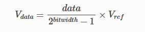
Voltage formula without attenuation:
Vdata = (data / (2^bitwidth - 1)) × Vref
Voltage formula with attenuation:
xxxxxxxxxxVdata = (data / (2^bitwidth - 1)) × Vref / k
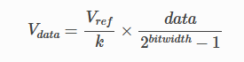
Parameter meanings:
| Parameter | Meaning |
|---|---|
data | ADC raw output code (12-bit: 0 ~ 4095) |
bitwidth | Resolution bit width (default 12) |
Vref | Reference voltage (3.3V) |
k | Attenuation coefficient (0dB=1, 2.5dB≈0.75, 6dB=0.5, 12dB=0.25) |
Calculation example — Input 2.2V, 12dB attenuation (k=0.25):
xxxxxxxxxxraw = (2.2V × 4095) / (3.3V / 0.25) ≈ 683
2.2 Bit Width and Resolution
xxxxxxxxxxtypedef enum { // Default, auto max bit width ADC_BITWIDTH_DEFAULT = 0, ADC_BITWIDTH_9 = 9, // 9-bit, 0~511 ADC_BITWIDTH_10 = 10, // 10-bit, 0~1023 ADC_BITWIDTH_11 = 11, // 11-bit, 0~2047 ADC_BITWIDTH_12 = 12, // 12-bit, 0~4095 (common) ADC_BITWIDTH_13 = 13, // 13-bit, 0~8191} adc_bitwidth_t;| Bit Width | Max Code | Min Resolution (Vref=3.3V) |
|---|---|---|
| 9 bit | 511 | ~6.5 mV |
| 10 bit | 1023 | ~3.2 mV |
| 11 bit | 2047 | ~1.6 mV |
| 12 bit (default) | 4095 | ~0.8 mV |
| 13 bit | 8191 | ~0.4 mV |
2.3 Attenuation Configuration
Attenuation determines the measurable voltage upper limit. Greater attenuation means larger range but lower effective resolution.
xxxxxxxxxxtypedef enum { ADC_ATTEN_DB_0 = 0, // No atten, range~1.1V ADC_ATTEN_DB_2_5 = 1, // 2.5dB atten, range~1.5V ADC_ATTEN_DB_6 = 2, // 6dB atten, range~2.2V ADC_ATTEN_DB_12 = 3, // 12dB atten, range~3.3V} adc_atten_t;| Attenuation Level | Coefficient k | Range (Vref=3.3V) |
|---|---|---|
ADC_ATTEN_DB_0 (0 dB) | ~1.00 | 0 ~ 1.1 V |
ADC_ATTEN_DB_2_5 (2.5 dB) | ~0.75 | 0 ~ 1.5 V |
ADC_ATTEN_DB_6 (6 dB) | ~0.50 | 0 ~ 2.2 V |
ADC_ATTEN_DB_12 (12 dB) | ~0.25 | 0 ~ 3.3 V |
2.4 Two Driver Modes
| Feature | One-shot Mode | Continuous + DMA Mode |
|---|---|---|
| Trigger Method | Manual single read | Auto continuous sampling |
| Data Transfer | CPU polling read | DMA auto-transfer |
| Speed | Low frequency (≤1kHz) | High frequency (up to MHz) |
| CPU Usage | High | Low |
| Use Case | Buttons, potentiometers, slow sensors | Audio, FFT, high-speed acquisition |
| Core API | adc_oneshot_read() | adc_continuous_start() |
This project uses one-shot mode, 16 times per second sampling and averaging, balancing response speed and stability.
3. ESP32-S3 ADC Hardware Characteristics
| Feature | Parameter |
|---|---|
| SAR ADC units | 2 (ADC1, ADC2) |
| Dedicated controllers | 5 (different scenarios: high performance/low power/power detection/peak detection) |
| Analog input pins | 18 |
| Internal channels | 1×VDD33, 2×PA_PKDET (some controllers) |
| Resolution | 9 / 10 / 11 / 12 / 13 bit configurable |
| DMA support | 1 controller supports |
| Multi-channel scan | 2 controllers support |
| Deep-sleep operation | 1 controller supports |
| ULP coprocessor | 2 controllers support |
Note: ADC2 shares resources with Wi-Fi. When Wi-Fi is enabled, ADC1 takes priority.
4. Project Architecture and Flow
xxxxxxxxxxapp_main()├─ adc_init() ← Initialize ADC handle & channel│ ├─ adc_oneshot_new_unit() Create ADC1 unit│ └─ adc_oneshot_config_channel() Configure channel: 12dB atten + 12-bit width│└─ adc_read_loop() ← Main loop (never returns)while(1):├─ for(16 times) adc_oneshot_read() → accumulate raw to sum├─ avg_raw = sum / 16 → calculate average├─ avg_mv = avg_raw × 3300 / 4095 → convert to mV├─ ESP_LOGI() print → avg_raw + mV└─ vTaskDelay(1000ms) → delay 1s
5. Hardware Dependencies
Hardware Connection: GPIO4 (ADC1_CH3) —待测电压 source (0~3.3V)
Dependencies: esp_adc, FreeRTOS, esp_log
6. Source Code Analysis
6.1 Header Files and Macro Configuration
x// 12dB atten→0~3.3V range// CH3 (GPIO4)// Samples per batch// Reference voltage (mV)// 12-bit full scale
// Log tagstatic const char *TAG = "ADC_DEMO";static adc_oneshot_unit_handle_t adc_handle;Why GPIO4 instead of GPIO3? ESP32-S3's GPIO3 is JTAG/USB-Serial-JTAG strapping pin, chip has internal pull-up resistor, ADC always reads 4095. Using GPIO4 (CH3) works normally.
6.2 adc_init() — Initialization
adc_init() does two things: Create ADC unit → Configure channel parameters.
adc_oneshot_new_unit()instantiates an ADC1 one-shot acquisition unit, returns handleadc_handle. All subsequent operations reference this unit through it.adc_oneshot_config_channel()binds GPIO4 (CH3) to this unit, while setting 12dB atten (range 0~3.3V) and default bit width (12-bit).
Called once, repeated calls don't reinitialize.
xxxxxxxxxxstatic void adc_init(void){    adc_oneshot_unit_init_cfg_t init_config = {        .unit_id = ADC_UNIT,                                    // ADC1    };    ESP_ERROR_CHECK(adc_oneshot_new_unit(&init_config, &adc_handle));
    adc_oneshot_chan_cfg_t chan_cfg = {        // 12dB atten        .atten = ADC_ATTEN,        // Default 12-bit        .bitwidth = ADC_BITWIDTH_DEFAULT,    };    ESP_ERROR_CHECK(adc_oneshot_config_channel(adc_handle, ADC_CHAN, &chan_cfg));}
6.3 adc_read_loop() — Acquisition Loop
adc_read_loop() is an infinite loop completing one sample → filter → print per second:
forloop callsadc_oneshot_read()16 times, each raw value accumulated tosum.sum / 16gets averageavg_raw, filtering high-frequency random noise.Formula
avg_raw × 3300 / 4095converts to millivolt valueavg_mv.ESP_LOGI()prints average raw and mV.vTaskDelay(1000ms)delays 1 second then next round.
This function has no return value (
while(1)never exits), it's the program's main loop.
xxxxxxxxxxstatic void adc_read_loop(void){    while (1)    {        // Accumulated sum        int sum = 0;
        for (int i = 0; i < SAMPLE_COUNT; i++)        {            int raw;            ESP_ERROR_CHECK(adc_oneshot_read(adc_handle, ADC_CHAN, &raw));            sum += raw;        }
        // Average        int avg_raw = sum / SAMPLE_COUNT;        int avg_mv = (avg_raw * ADC_VREF_MV) / ADC_MAX_COUNT;   // mV = raw × 3300 / 4095
        // Print: ADC raw value + voltage (mV)        ESP_LOGI(TAG, "ADC_Value=%4d, Voltage=%4d mV", avg_raw, avg_mv);
        // 1 second interval        vTaskDelay(pdMS_TO_TICKS(1000));    }}
Mean filtering is the simplest digital filtering. No need for complex algorithms like EMA/Kalman. After 16-time averaging, ±3~5 LSB inherent noise is compressed to ±1 LSB, with only 1 second response delay.
6.4 app_main() — Main Entry
xxxxxxxxxxFunction signature: void app_main(void)Input: NoneOutput: None
xxxxxxxxxxvoid app_main(void){ adc_init() → Initialize ADC adc_read_loop() → Loop acquisition and print}7. Operation Flow
7.1 Build and Flash
For detailed flashing process, see: 1. Before Development → 3. Build and Flash
7.2 Normal Acquisition
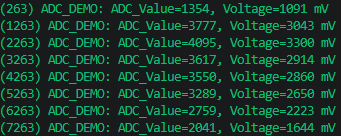
Log field meanings:
| Field | Example | Meaning |
|---|---|---|
I | I | INFO level log |
(1263) | 1263 | Milliseconds since system startup (timestamp) |
ADC_DEMO | ADC_DEMO | Log tag (TAG macro defined in code) |
ADC_Value=3777 | 3777 | ADC raw value average of 16 samples (0~4095) |
Voltage=3043 | 3043 | Converted measured voltage in mV (i.e., 3.043V) |
Conversion:
mV = ADC_Value × 3300 / 4095. WhenADC_Value=3777, Voltage=3300 × 3777 / 4095 ≈ 3043mV.
xxxxxxxxxxI (1263) ADC_DEMO: ADC_Value=3777, Voltage=3043 mVI (2263) ADC_DEMO: ADC_Value=4095, Voltage=3300 mVI (3263) ADC_DEMO: ADC_Value=3617, Voltage=2914 mVI (4263) ADC_DEMO: ADC_Value=3550, Voltage=2860 mVI (5263) ADC_DEMO: ADC_Value=3289, Voltage=2650 mVI (6263) ADC_DEMO: ADC_Value=2759, Voltage=2223 mV
7.2 Boundary Cases
Boundary cases are quick self-checks to verify ADC hardware and code are normal:
Connect GND → reads 0: Pin pulled to 0V, ADC reads minimum code 0, indicates ADC zero point is normal.
Connect 3.3V → reads 4094: Pin connected to reference voltage, reads near full scale (±1 LSB error is normal), indicates ADC full scale is normal.
Pin floating → readings jump randomly: Floating pin acts like an antenna, couples surrounding EM fields (50Hz mains, Wi-Fi signals, etc.). SAR ADC sampling injects charge into pin without release path, readings drift randomly—this is normal phenomenon, not a hardware fault.
Verification method: Zero point normal + full scale normal = hardware and code are fine. Floating readings are physical phenomenon, not a bug.
xxxxxxxxxx// Pin connected to GNDI (144263) ADC_DEMO: ADC_Value=0, Voltage=0 mV// Pin to 3.3VI (285263) ADC_DEMO: ADC_Value=4095, Voltage=3300 mV// Pin floating, antenna effect, randomI (6263) ADC_DEMO: ADC_Value=2759, Voltage=2223 mV // DriftingI (7263) ADC_DEMO: ADC_Value=2041, Voltage=1644 mV // Continue drifting
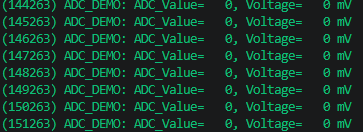
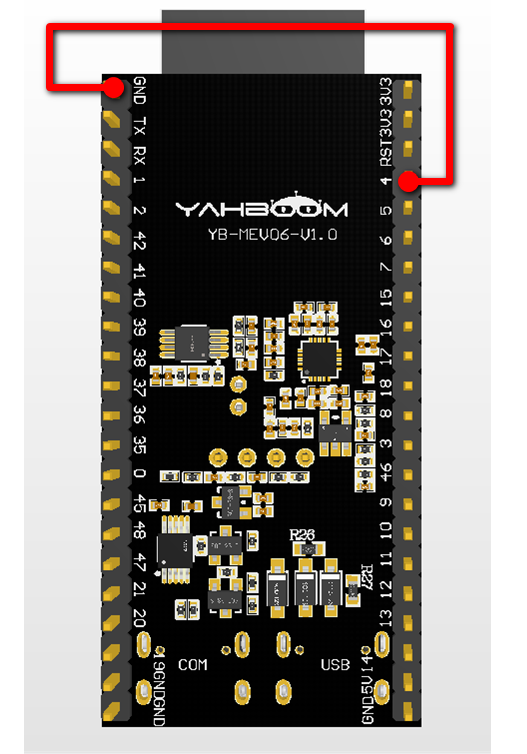
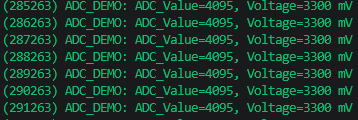
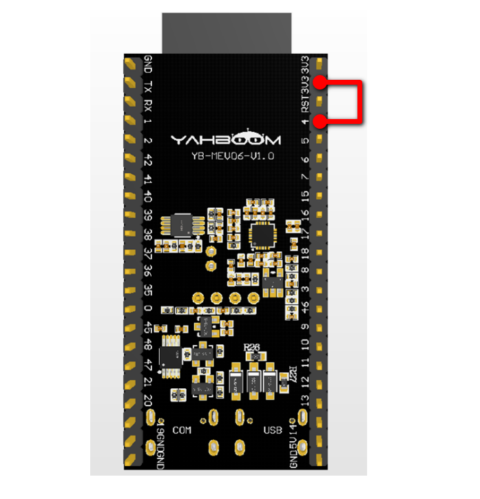
Floating pin readings first increase then decrease is normal phenomenon, reason:
SAR ADC injects charge into pin during sampling, floating has no release path, parasitic capacitor voltage accumulates
50Hz mains electric field coupling, manifests as low-frequency sinusoidal drift
Solution: Connecting to GND returns to zero = code is fine
8. Common Issues
| Phenomenon | Cause | Solution |
|---|---|---|
| Reading always 4095 | Pin floating / using strapping pins (GPIO0/3/45/46) | Connect to GND to verify zero → use GPIO4 or other normal pins |
| Reading always 0 | Pin shorted to GND / atten configuration error | Check wiring, confirm input voltage within range |
| Reading ±3~5mV jitter | Normal, ADC inherent quantization noise | Average multiple samples (built-in 16-time average) |
| Large reading drift | Pin floating | Connect pull-down resistor (10kΩ→GND) or actual signal |
| ADC2 + Wi-Fi abnormal | ADC2 shares resources with Wi-Fi | Use ADC1 instead |
| Strapping pins read 4095 | Internal pull-up raises level | Avoid GPIO0, GPIO3, GPIO45, GPIO46 |