Welcome to ESP32 Core Board repository
2. I2C_OLED Display Experiment
I2C_OLED Display Experiment
I2C_OLED Display Experiment1. I2C OLED Overview2. Core Concepts2.1 I2C Bus Principle2.1.1 Standard I2C Write Sequence (General Format)2.1.2 SSD1306 I2C Write Sequence (Actual Format for This Project)2.1.3 Segment-by-Segment Analysis2.1.4 Complete I2C Single Byte Transmit Process (Code Level)2.1.5 Speed Modes2.2 SSD1306 Display Principle2.3 Font Storage Format3. ESP32-S3 I2C Hardware Specifications4. Project Architecture and Flow5. Hardware Dependencies6. Source Code Details6.1 oled_bus.c — I2C Bus Initialization6.2 oled.c — Low-level Command/Data Sending6.3 ssd1306_init() — Controller Initialization6.4 oled_render_page() — Row-major Transpose Rendering6.5 app_main() — Entry Point7. Operation Flow7.1 Build and Flash Process7.2 Normal Display8. FAQ
1. I2C OLED Overview
I2C (Inter-Integrated Circuit) is a synchronous serial communication protocol that requires only SDA (data line) + SCL (clock line) two signal lines for bidirectional communication between MCU and multiple peripherals.
This project drives an OLED display (128×32 pixels) with SSD1306 controller via I2C to implement character display functionality.
Typical use cases:
| Scenario | Description |
|---|---|
| Embedded Device Info Screen | Display device status, IP address, sensor readings |
| Smart Wearables | Small size, low power real-time information display |
| Instrumentation | Thermometer, multimeter, and other small displays |
| Human-Machine Interface | Simple menus, parameter setting interfaces |
2. Core Concepts
2.1 I2C Bus Principle
The I2C bus implements "wire-AND" logic through open-drain output + pull-up resistor: the bus is default pulled to high level by pull-up resistors. Any device can pull the bus low through internal NMOS, avoiding short circuit when one device outputs high and another outputs low.
2.1.1 Standard I2C Write Sequence (General Format)
The vast majority of I2C devices (sensors, EEPROM, etc.) follow a unified format for single-byte write:
xSequence: START → DevAddr(7b)+W → ACK → RegAddr(8b) → ACK → Data(8b) → ACK → STOP├─── address frame ───┤ACK├── register address ──┤ACK├─── data ───┤ACK│ 8-bit │ │ 8-bit │ │ 8-bit │SCL: ──┐┌┐┌┐┌┐┌┐┌┐┌┐┌┐┌┐┌┐┌┐┌┐┌┐┌┐┌┐┌┐┌┐┌┐┌┐┌┐┌┐┌┐┌┐┌┐┌┐┌┐┌┐┌┐┌──
Standard I2C write sequence: START → device address+R/W → ACK → register address → ACK → data → ACK → STOP. "Register address" tells the slave which internal register to write to, "data" is the value to write. SCL has 27 clock cycles (3×9), SDA changes at SCL low level and is sampled at SCL high level.
2.1.2 SSD1306 I2C Write Sequence (Actual Format for This Project)
SSD1306 does not have traditional register addresses. Instead, it uses a control byte to distinguish whether subsequent bytes are commands or data. The control byte occupies the position of "register address" in standard I2C:
xxxxxxxxxxStandard I2C: DevAddr+R/W → ACK → register address → ACK → data → ACK → STOPSSD1306: DevAddr+R/W → ACK → control byte → ACK → cmd/data → ACK → STOP(0x00=command)(0x40=data)
Taking sending a command as an example (oled_cmd(c)):
xxxxxxxxxxSequence: START → 0x78(Addr+W) → ACK → 0x00(Ctrl:command) → ACK → CmdByte → ACK → STOP├──── address frame ────┤ACK├─── control byte ───┤ACK├── command byte ──┤ACK│ 0x78=write address │ │ 0x00=command mode │ │ command value │SCL: ──┐┌┐┌┐┌┐┌┐┌┐┌┐┌┐┌┐┌┐┌┐┌┐┌┐┌┐┌┐┌┐┌┐┌┐┌┐┌┐┌┐┌┐┌┐┌┐┌┐┌┐┌┐┌┐┌┐┌┐┌──Each segment's 8-bit data transmitted on SDA (each byte followed by 1-bit ACK):Address frame: 1 1 1 1 1 0 0 0 (→ ACK) corresponds to 0x78 = 0x3C<<1 | W=0Control byte: 0 0 0 0 0 0 0 0 (→ ACK) corresponds to 0x00 = next byte is commandCommand byte: x x x x x x x x (→ ACK) corresponds to command value, e.g. 0xAF = Display ON
SSD1306's control byte (0x00/0x40) occupies the position of standard device "register address" in I2C sequence, but the meaning is different — it identifies whether subsequent bytes are commands or data, not pointing to some internal register.
2.1.3 Segment-by-Segment Analysis
① Start Condition
xxxxxxxxxxSCL: ───────────┐│SDA: ─────────┐ ││ │└─┘
When SCL is high, SDA goes from high to low → START. Bus transitions from idle to busy, all slaves start listening for addresses.
② Address Frame
The first byte sent by master = 7-bit slave address + 1-bit read/write direction:
xxxxxxxxxxBit: 7 6 5 4 3 2 1 0┌───┬───┬───┬───┬───┬───┬───┬───┐│ 1 │ 1 │ 1 │ 1 │ 0 │ 0 │ 0 │ R/W│└───┴───┴───┴───┴───┴───┴───┴───┘└────────── 0x3C ─────────┘ └┬─┘0=write,1=read
Complete 8-bit address byte =
0x3C << 1 | 0= 0x78 (write) or0x3C << 1 | 1= 0x79 (read)SSD1306 only receives commands and data, no readback provided, so R/W is always 0 (write)
③ Acknowledge Bit (ACK / NACK)
xxxxxxxxxx9th clock┌──┐SCL: ────┘ └───┌──────┐SDA: ───┘ └─── ← Slave pulls low = ACK
After every 8-bit transfer, the receiver must pull SDA low during the 9th SCL clock cycle as ACK. If no ACK (SDA stays high = NACK), master should stop or retry.
The 9 SCL pulses are generated by the master, but the SDA level during the 9th clock is controlled by the receiver (master releases SDA, slave pulls it low).
④ Data Frame
Same format as address frame: 8-bit data + 1-bit ACK. SSD1306 data frames are divided into two types:
| Data Byte | Prefix | Meaning |
|---|---|---|
0x00 + command byte | Control byte = 0x00 | Subsequent bytes are SSD1306 commands |
0x40 + data byte | Control byte = 0x40 | Subsequent bytes are GDDRAM display data |
SSD1306 does not support pure I2C standard command/data distinction, but uses the first data byte (Co=0, D/C#=0/1) as control identifier, followed by the actual command or data value. This is an SSD1306-specific convention, not the I2C protocol standard.
⑤ Stop Condition
xxxxxxxxxxSCL: ┌──────────┘SDA: ──────┐└────
When SCL is high, SDA goes from low to high → STOP. Bus is released, returns to idle state.
2.1.4 Complete I2C Single Byte Transmit Process (Code Level)
oled_cmd() sends a single command byte with complete steps:
xxxxxxxxxxSTART → 0x78 → ACK(slave) → 0x00 → ACK(slave) → command → ACK(slave) → STOPMaster actions:i2c_master_transmit(oled_dev, {0x00, cmd_byte}, 2, -1)↑ ↑control byte command byte
Corresponding code implementation (oled.c:oled_cmd):
xxxxxxxxxxvoid oled_cmd(uint8_t c){ // [Ctrl byte, Cmd byte] uint8_t buf[2] = {0x00, c}; i2c_master_transmit(oled_dev, buf, 2, -1); // ↑ ESP-IDF driver automatically completes START→address→ACK→buf[0]→ACK→buf[1]→ACK→STOP}ESP-IDF's
i2c_master_transmit()encapsulates the low-level sequence: automatically sends START, address frame, waits for ACK, sends bytes one by one with ACK, finally sends STOP. Developer only needs to care about the byte content to send.
2.1.5 Speed Modes
| Mode | Clock Frequency | Use Case |
|---|---|---|
| Standard (Sm) | 100 kHz | Traditional low-speed devices |
| Fast (Fm) | 400 kHz | Common mode, this example |
| Fast Plus (Fm+) | 1 MHz | High-speed sensors |
| High Speed (Hs) | 3.4 MHz | Requires special master support |
2.2 SSD1306 Display Principle
SSD1306 divides the 128×32 pixel OLED panel into 4 "pages" (Page 0~3), each page 8 rows of pixels:
xxxxxxxxxxPage 0 ← Physical top (rows 0~7)Page 1 ← Rows 8~15Page 2 ← Rows 16~23Page 3 ← Physical bottom (rows 24~31)
Each byte of data sent (0x40 + 8-bit) corresponds to 8 vertical pixels in one column — bit 0 at top, bit 7 at bottom. After writing, column address auto-increments, allowing continuous writing of a full page (128 columns).
xxxxxxxxxxCol0 Col1 Col2 ... Col127Page0: ■□□ ■□■ □□□ □■□□■□ □■□ □□□ ■□□......(8 rows total)......Page1: ...and so on...
2.3 Font Storage Format
This project supports 4 font types, divided into two storage formats:
Row-major: Each uint16_t = one row of pixels, FontHeight entries = one character. During rendering, transpose (row→column) is required to write to SSD1306's page memory.
Column-major: Each uint16_t = one column, high byte = upper 8px (Page0), low byte = lower 8px (Page1). No transpose needed, direct write.
| Font | Size | Entries per Character | Storage Format |
|---|---|---|---|
| Font7x10 | 7×10 | 10 | Row-major |
| Font11x18 | 11×18 | 18 | Row-major |
| Font16x26 | 16×26 | 26 | Row-major |
| Font16x16 | 16×16 | 32 | Column-major |
3. ESP32-S3 I2C Hardware Specifications
| Feature | Parameter |
|---|---|
| I2C Controller Count | 2 (I2C0, I2C1) |
| Speed Modes | Standard (100kHz), Fast (400kHz), Fast+ (1MHz) |
| Addressing Modes | 7-bit and 10-bit |
| FIFO Depth | 32 bytes |
| DMA Support | Supported |
| Internal Pull-up | Optional (enabled in this example, no external resistor needed) |
4. Project Architecture and Flow
Three-layer architecture:
xxxxxxxxxxmain.c (Application Layer)└─ app_main()├─ i2c_init() Initialize I2C bus, mount 0x3C device├─ ssd1306_init() Send SSD1306 initialization sequence├─ oled_clear() Clear screen└─ oled_show_str() Display stringoled_bus.c (Bus Layer)└─ i2c_init()├─ i2c_new_master_bus() Create I2C master (SDA=41, SCL=42, 400kHz)└─ i2c_master_bus_add_device() Mount OLED device (address 0x3C)oled.c (Driver Layer)├─ oled_cmd() / oled_data() Send command/data via I2C├─ ssd1306_init() 29 command initialization sequence├─ oled_clear() 4 pages × 128 columns write 0x00└─ oled_show_str() Iterate string, call font rendering function└─ oled_render_page() Row-major → column transpose → write to GDDRAM
5. Hardware Dependencies
Hardware Connection:
| Signal | GPIO | Description |
|---|---|---|
| SDA | 41 | I2C data line |
| SCL | 42 | I2C clock line |
| OLED Address | 0x3C | 7-bit I2C address |
| Resolution | 128×32 | SSD1306 controller |
Internal pull-up is enabled, no external pull-up resistor needed.
Required Components: driver/i2c_master, FreeRTOS
6. Source Code Details
6.1 oled_bus.c — I2C Bus Initialization
i2c_init() creates I2C master bus, mounts SSD1306 device at address 0x3C in 400kHz Fast Mode, and stores the device handle in global variable oled_dev for all driver layer functions to reference.
xxxxxxxxxx// I2C data line// I2C clock linei2c_master_dev_handle_t oled_dev;
void i2c_init(void){ i2c_master_bus_config_t bus_cfg = { .sda_io_num = I2C_SDA, .scl_io_num = I2C_SCL, .clk_source = I2C_CLK_SRC_DEFAULT, // Enable internal pull-up .flags.enable_internal_pullup = 1, };
i2c_master_bus_handle_t bus; // Create master bus i2c_new_master_bus(&bus_cfg, &bus);
i2c_device_config_t dev_cfg = { .device_address = OLED_ADDR, .scl_speed_hz = 400000, // 400kHz Fast mode };
// Attach OLED device i2c_master_bus_add_device(bus, &dev_cfg, &oled_dev);}6.2 oled.c — Low-level Command/Data Sending
SSD1306 distinguishes command (0x00) and data (0x40) through I2C prefix byte:
xxxxxxxxxx// Send single-byte commandvoid oled_cmd(uint8_t c){    // [Control byte, Command byte]    uint8_t buf[2] = {0x00, c};    i2c_master_transmit(oled_dev, buf, 2, -1);    // Blocking send}
// Send single-byte datavoid oled_data(uint8_t d){    // [Control byte, Data byte]    uint8_t buf[2] = {0x40, d};    i2c_master_transmit(oled_dev, buf, 2, -1);    // Blocking send}
6.3 ssd1306_init() — Controller Initialization
SSD1306 requires configuring internal registers in a specific sequence after power-on. The initialization sequence has 29 commands, key registers as follows:
| Register | Value | Function |
|---|---|---|
| 0xAE / 0xAF | — | Display OFF / ON |
| 0xD5 | 0x80 | Clock divide ratio, default frequency |
| 0xA8 | 0x1F | MUX ratio = 32 (0x1F = 31) |
| 0x8D | 0x14 | Charge pump enable, enable internal DC-DC |
| 0x20 | 0x02 | Page addressing mode |
| 0xA1 | — | Segment remap (horizontal flip) |
| 0xC0 | — | COM scan direction (normal) |
| 0xDA | 0x12 | COM pin hardware configuration (128×32 must be 0x12) |
xxxxxxxxxxvoid ssd1306_init(void){    vTaskDelay(100);     // Wait for power stable
    oled_cmd(0xAE);      // Display OFF    oled_cmd(0xD5); oled_cmd(0x80);  // Set clock divide    oled_cmd(0xA8); oled_cmd(0x1F);  // MUX = 32 (0x1F = 31)    oled_cmd(0xD3); oled_cmd(0x00);  // Display offset = 0    oled_cmd(0x40);                   // Start line = 0    oled_cmd(0x8D); oled_cmd(0x14);  // Charge pump enable    oled_cmd(0x20); oled_cmd(0x02);  // Page addressing mode    // Segment remap (horizontal flip)    oled_cmd(0xA1);    oled_cmd(0xC0);    oled_cmd(0xDA); oled_cmd(0x12);    oled_cmd(0x81); oled_cmd(0xCF);  // Set contrast    oled_cmd(0xD9); oled_cmd(0xF1);  // Pre-charge period    oled_cmd(0xDB); oled_cmd(0x40);  // VCOMH level    oled_cmd(0x2E);                   // Stop scroll    oled_cmd(0xA4);                   // Entire display ON    // Normal display (non-inverted)    oled_cmd(0xA6);
    // Clear screen, remove noise    oled_clear();
    oled_cmd(0xAF);      // Display ON    vTaskDelay(100);     // Wait for display stable}
6.4 oled_render_page() — Row-major Transpose Rendering
Row-major font needs transpose to vertical column data before writing to SSD1306. Core logic: for rows in the specified range (start_row ~ start_row+row_count-1), traverse each column to extract bits, combine into one byte of vertical column data.
xxxxxxxxxx// Row-major glyph bit extractstatic void oled_render_page(uint8_t x, const uint16_t *data, int width, int start_row, int row_count, int page){ // Set page + column address oled_set_pos(page, x); for (int col = 0; col < width; col++) { uint8_t byte = 0; for (int r = 0; r < row_count; r++) { if (GLYPH_BIT(data, start_row + r, col)) // Row bit → vertical bit (MSB=top) byte |= (1 << (row_count - 1 - r)); } // Write one column of 8 pixels oled_data(byte); }}6.5 app_main() — Entry Point
app_main() sequentially: I2C bus init → SSD1306 controller init → clear screen → select 16×26 font → show "YAHBOOM" at x=0.
xxxxxxxxxxvoid app_main(void){ // 1. Init I2C bus i2c_init(); // 2. Init SSD1306 controller ssd1306_init(); oled_clear(); // 3. Clear screen // 4. Select 16x26 font oled_set_font(OLED_FONT_SEL_16X26); oled_show_str(0, "YAHBOOM"); // 5. Show string}7. Operation Flow
7.1 Build and Flash Process
For detailed flash process: 1. Before Development → 3. Build and Flash
7.2 Normal Display
After flashing, OLED screen displays "YAHBOOM" in the center (16×26 large font). Font and content can be changed by modifying oled_set_font() and oled_show_str().
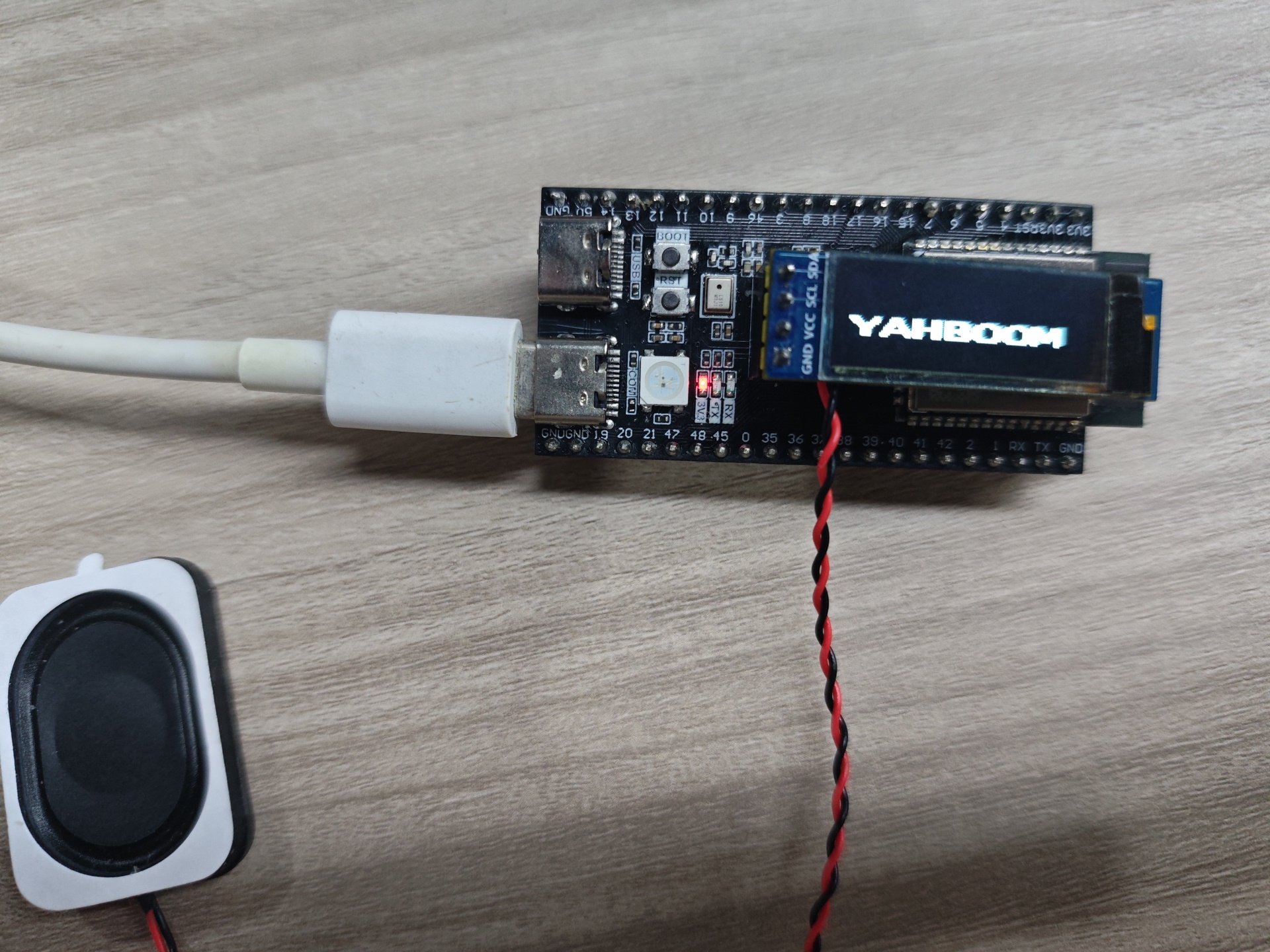
The following example shows how to switch fonts and display text. Uncomment to preview each of the 4 fonts.
xxxxxxxxxxoled_clear(); // Clear screen// 11×18 fontoled_set_font(OLED_FONT_SEL_11X18); oled_show_str(0, "0: 11x18");// 16×26 fontoled_set_font(OLED_FONT_SEL_16X26); oled_show_str(0, "1: 16x26");// 7×10 fontoled_set_font(OLED_FONT_SEL_7X10); oled_show_str(0, "2: 7x10");// 16×16 fontoled_set_font(OLED_FONT_SEL_16X16); oled_show_str(0, "3: 16x16");8. FAQ
| Symptom | Cause | Solution |
|---|---|---|
| Screen all black, no display | I2C wiring error / address mismatch / no power | Check SDA=GPIO41, SCL=GPIO42 wiring, confirm module VCC=3.3V, GND connected |
| Screen garbled / random noise | Initialization sequence sending abnormal or power-on unstable | Check if I2C pull-up is enabled (enable_internal_pullup = 1), repower |
| Display content offset/misaligned | Page addressing mode not correctly configured or column start position wrong | Confirm 0x20→0x02 (page addressing) in ssd1306_init() is correctly sent |
| Screen flickering | I2C clock too high or signal quality poor | Lower scl_speed_hz from 400000 to 100000 for testing |
| Font display incomplete | Font compile macros not enabled | Check if corresponding OLED_FONT_* macros are defined in oled_fonts.h |
| No display after USB connected | GPIO41/42 may be multiplexed by USB or PSRAM | ESP32-S3's GPIO41/42 on some boards are multiplexed with USB, check board pin assignment |