Welcome to ESP32 Core Board repository
3. SPI Bus Communication
SPI Bus Communication Experiment
SPI Bus Communication Experiment1. SPI Bus Communication Overview2. Core Concepts2.1 SPI Four-Wire Signals2.2 SPI Modes (CPOL & CPHA)2.3 Full-Duplex Characteristic2.4 SPI Modes Summary2.5 Arduino Master vs ESP-IDF Slave3. Hardware Dependencies4. Project Architecture and Flow5. Source Code5.1 Master — SPI Initialization and Transfer5.2 Slave — DMA Buffer and Initialization5.3 Slave — Blocking Wait for Transfer6. Operation Flow6.1 Compile and Flash6.2 Normal Phenomena6.3 Verification Methods7. Common Issues
1. SPI Bus Communication Overview
SPI (Serial Peripheral Interface) is a four-wire full-duplex synchronous serial bus (SCK/MOSI/MISO/CS), with speed far exceeding UART and I2C.
This experiment uses two ESP32-S3 boards to build SPI master-slave communication: the master sends strings via SPIClass (Arduino API), and the slave receives and replies via spi_slave driver (ESP-IDF Native API), demonstrating SPI full-duplex transmission, manual CS control, and DMA buffer configuration.
Why two boards are needed: A single Arduino cannot simultaneously act as both master and slave on the same SPI bus, hardware peripheral architecture does not support it.
The most intuitive way to verify the complete SPI transmit/receive process is:
Board A as master, Board B as slave, send and receive data to/from each other, and observe the serial port print results.
Typical Application Scenarios:
| Application Type | Examples |
|---|---|
| High-speed peripherals | TFT/OLED screens, SD cards, SPI Flash |
| Sensors | High-precision ADC/DAC, IMU gyroscope |
| Inter-board communication | Dual MCU high-speed data exchange |
| Display drivers | ePaper ink screen, LED matrix |
2. Core Concepts
2.1 SPI Four-Wire Signals
| Signal | Direction (Master perspective) | Function |
|---|---|---|
| SCK | Output | Clock, generated by master |
| MOSI | Output | Master Out Slave In — master sends to slave |
| MISO | Input | Master In Slave Out — slave sends to master |
| CS | Output | Chip select, active low to select target slave |
2.2 SPI Modes (CPOL & CPHA)
SPI has 4 modes, determined by CPOL (Clock Polarity) and CPHA (Clock Phase):
| Mode | CPOL | CPHA | SCK Idle Level | Sampling Edge |
|---|---|---|---|---|
| 0 | 0 | 0 | Low | Rising edge |
| 1 | 0 | 1 | Low | Falling edge |
| 2 | 1 | 0 | High | Falling edge |
| 3 | 1 | 1 | High | Rising edge |
This example uses Mode 0 (CPOL=0, CPHA=0), SCK idle low level, sampling on rising edge. Both master and slave must be set to the same mode.
2.3 Full-Duplex Characteristic
During each SPI clock pulse, two things happen simultaneously: the master outputs 1 bit on MOSI while sampling 1 bit on MISO. Therefore, for every byte the master sends, it inevitably receives one byte — even if the slave didn't prepare meaningful data. This is not a bug, it's a hardware characteristic.
Key slave constraint: Because the master controls the clock, the slave must have the reply data filled into tx_buf before the master initiates transmission. Once CS goes low and SCK starts running, the slave has no choice — each clock cycle it must drop one bit onto MISO.
2.4 SPI Modes Summary
SPI has 4 modes (determined by CPOL and CPHA). This experiment uses SPI_MODE0: SCK idle is low level, data is sampled on the first edge (rising edge). Both master and slave modes must match.
2.5 Arduino Master vs ESP-IDF Slave
| Master (Arduino) | Slave (ESP-IDF Native) | |
|---|---|---|
| API | SPIClass + spi.transfer() | spi_slave_initialize() + spi_slave_transmit() |
| Controller | SPI3_HOST | SPI2_HOST |
| DMA | Automatic management | Manual declaration DRAM_ATTR + 4-byte alignment |
3. Hardware Dependencies
This experiment requires two ESP32-S3 boards, one flashed with master program, one with slave program.
Master pins:
| Pin | Peripheral | Configuration | Description |
|---|---|---|---|
| GPIO4 | SCK | SPI clock output | Connected to slave GPIO4 |
| GPIO5 | MOSI | Master output | Connected to slave GPIO5 |
| GPIO6 | MISO | Master input | Connected to slave GPIO6 |
| GPIO2 | CS | Manual chip select | Connected to slave GPIO2 (active low) |
| GND | GND | Common ground between master and slave | Connected to slave GND |
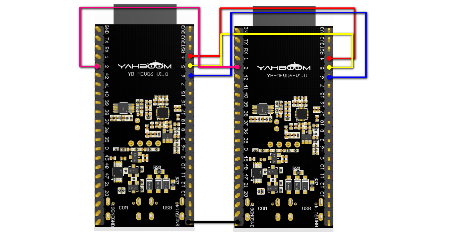
Slave pins: Identical to master, connected one-to-one.
ESP32-S3 SPI Hardware Features:
| Feature | Parameter |
|---|---|
| Number of SPI controllers | 4 (SPI0/SPI1 occupied by Flash/PSRAM, SPI2/SPI3 available for user) |
| Operating modes | Master / Slave |
| Maximum clock frequency | 80MHz (master mode), 20MHz (slave mode) |
| Data width | 1/2/4/8 wire (Standard/DUAL/QUAD/OCTAL) |
| FIFO depth | 64 bytes (independent TX/RX) |
| DMA support | Yes (slave must place buffer in DRAM with 4-byte alignment) |
| GPIO mapping | Any GPIO configurable as SPI pin via IO MUX |
| SPI modes | 0/1/2/3 (CPOL + CPHA combination), this experiment uses MODE0 |
Requires two ESP32-S3 boards, 4 Dupont wires connecting SCK/MOSI/MISO/CS, plus one GND wire for common ground.
4. Project Architecture and Flow
x[Master] setup()├─ SPI.begin(SCK, MISO, MOSI, -1) // -1 = manual CS control├─ pinMode(CS, OUTPUT); CS=HIGH // Idle: release slave└─ Toggle CS 3 times to verify wiring[Master] loop()├─ Construct "Hello N from Master!"├─ CS=LOW → beginTransaction → Loop transfer(BUF_SIZE bytes) → endTransaction → CS=HIGH└─ Print TX and RX results via serial[Slave] setup()├─ spi_slave_initialize(SPI2_HOST, ...) // Configure bus + slave interface└─ Pre-fill tx_buf = "Slave Received, over"[Slave] loop()├─ Block waiting for master transmission (spi_slave_transmit)├─ Print TX/RX content└─ Construct next reply based on received content → Loop
5. Source Code
Source Code Location:
Source code → Arduino → 2.Serial communication → 3. SPI → SPI_Master → SPI_Master.ino
5.1 Master — SPI Initialization and Transfer
Using manual CS control to precisely control chip select timing before and after transfer.
xxxxxxxxxxSPIClass spi(1);  // SPIClass(1) = SPI3_HOST
void setup() {  spi.begin(PIN_SCK, PIN_MISO, PIN_MOSI, -1);  // -1 = no hardware CS  pinMode(PIN_CS, OUTPUT);  digitalWrite(PIN_CS, HIGH);  // Idle: don't select slave}
void loop() {  digitalWrite(PIN_CS, LOW);                    // ① Select slave  spi.beginTransaction(SPISettings(100000, MSBFIRST, SPI_MODE0));  for (int i = 0; i < BUF_SIZE; i++)    rx[i] = spi.transfer(tx[i]);                // ② Full-duplex TX/RX  spi.endTransaction();  digitalWrite(PIN_CS, HIGH);                   // ③ Release slave}
Each call to
spi.transfer(tx_byte)completes 8 SCK clock cycles: sending 8 bits to MOSI while sampling 8 bits from MISO.
5.2 Slave — DMA Buffer and Initialization
DMA buffers must be in internal DRAM with 4-byte alignment.
xxxxxxxxxxstatic uint8_t DRAM_ATTR tx_buf[64] __attribute__((aligned(4)));static uint8_t DRAM_ATTR rx_buf[64] __attribute__((aligned(4)));
void setup() {  spi_bus_config_t bus_cfg = {};  bus_cfg.mosi_io_num = PIN_MOSI;  bus_cfg.miso_io_num = PIN_MISO;  bus_cfg.sclk_io_num = PIN_SCK;
  spi_slave_interface_config_t slv_cfg = {};  slv_cfg.mode = 0;               // SPI_MODE0  slv_cfg.spics_io_num = PIN_CS;
  spi_slave_initialize(SPI2_HOST, &bus_cfg, &slv_cfg, SPI_DMA_CH_AUTO);  strcpy((char*)tx_buf, "Slave Received, over");  // Pre-fill first reply}
DRAM_ATTRplaces the array in internal DRAM (DMA can only access internal RAM, not PSRAM).__attribute__((aligned(4)))ensures 4-byte alignment, otherwise DMA triggers hardware exceptions.
5.3 Slave — Blocking Wait for Transfer
spi_slave_transmit() blocks the current task until the master initiates transfer or timeout.
xxxxxxxxxxvoid loop() {  memset(rx_buf, 0xAA, BUF_SIZE);   // Fill with marker value
  spi_slave_transaction_t t = {};  t.length    = BUF_SIZE * 8;       // Unit is bits! 64 bytes = 512 bits  t.tx_buffer = tx_buf;  t.rx_buffer = rx_buf;
  esp_err_t ret = spi_slave_transmit(SPI2_HOST, &t, pdMS_TO_TICKS(3000));
  // Prepare next reply based on received content  snprintf((char*)tx_buf, BUF_SIZE, "I got: %s", (char*)rx_buf);}
t.lengthunit is bits, not bytes — this is the most commonly miswritten field inspi_slave_transaction_t. The0xAAfill pattern forrx_bufallows visual inspection of how many bytes the master actually sent.
6. Operation Flow
6.1 Compile and Flash
Arduino Flash Process: See 1. Before Development → 2. Build and Flash.
Connect the two boards pin-to-pin according to the pin table with Dupont wires, must share common ground
Compile and flash
SPI_Master.inoandSPI_Slave.inoto the respective boards
6.2 Normal Phenomena
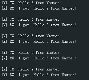
Master serial monitor (115200 bps) prints every second:
xxxxxxxxxx[M] TX: Hello 0 from Master![M] RX: Slave Received, over[M] TX: Hello 1 from Master![M] RX: I got: Hello 1 from Master!
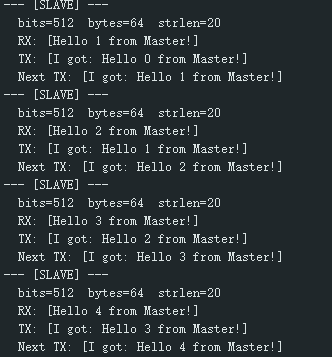
xxxxxxxxxx--- [SLAVE] ---bits=512 bytes=64 strlen=20RX: [Hello 1 from Master!]TX: [I got: Hello 0 from Master!]Next TX: [I got: Hello 1 from Master!]--- [SLAVE] ---bits=512 bytes=64 strlen=20RX: [Hello 2 from Master!]TX: [I got: Hello 1 from Master!]Next TX: [I got: Hello 2 from Master!]
6.3 Verification Methods
| Operation | Expected Result |
|---|---|
| Power on both boards | Master RX receives slave reply |
| Remove any one signal wire | Master RX is all 0 or garbled |
| Master and slave SPI modes don't match | Data byte offset or all wrong |
7. Common Issues
| Phenomenon | Cause | Solution |
|---|---|---|
| Master RX is all 0xAA | Slave not running or CS not connected | Confirm slave is powered on, check CS wiring |
| Master RX data misaligned | SPI mode mismatch | Both master and slave use SPI_MODE0 |
Slave spi_slave_transmit timeout | CS or SCK wiring broken | Use multimeter to check each wire |
| Slave DMA exception | Buffer not aligned or not in DRAM | Confirm DRAM_ATTR + __attribute__((aligned(4))) |
| Garbage bytes in data | Dupont wires too long causing signal reflection | Lower SCK frequency or shorten Dupont wires |